IPC-TM-650 EN 2022 试验方法.pdf - 第497页
1 Scope This test method describes procedure for measur- ing dielectric permittivity and loss tangent of embedded pas- sive materials. The measurements are made in an APC-7 coaxial configuration where the test specimen r…

3330
!**** END CALIBRATION OF UNIT ****
3340 !
3400 !**** OPEN 16453A FIXTURE MEASUREMENT ****
3410 ON INTR Scode GOTO Open_end1
3420 OUTPUT @Hp4291;‘‘*CLS;*OPC?’’
3430 ENTER @Hp4291;Opc
3440 INPUT ‘‘CONNECT FIXTURE AND LOCK GAP OPEN,
THEN PRESS [RETURN OR x1]’’,A$
3460 ENABLE INTR Scode;2
3470 OUTPUT @Hp4291;‘‘SENS:CORR2:COLL STAN4’’
3480 Wait_open1:GOTO Wait_open1
3490 Open_end1:!
3500 !
3600 !**** 16453A FIXTURE SHORT MEASUREMENT ****
3610 ON INTR Scode GOTO Short_end1
3620 OUTPUT @Hp4291;‘‘*CLS;*OPC?’’
3630 ENTER @Hp4291;Opc
3640 INPUT ‘‘CLOSE AND SHORT FIXTURE GAP, THEN
PRESS [RETURN OR x1]’’,A$
3650 ENABLE INTR Scode;2
3660 OUTPUT @Hp4291;‘‘SENS:CORR2:COLL STAN5’’
3670 Wait_short1:GOTO Wait_short1
3680 Short_end1:!
3690 !
3800 !**** TEFLON LOAD IN 16453A MEASUREMENT ****
3810 ON INTR Scode GOTO Load_end1
3820 OUTPUT @Hp4291;‘‘*CLS;*OPC?’’
3830 ENTER @Hp4291;Opc
3840 INPUT ‘‘PLACE TEFLON STANDARD INTO FIXTURE,
THEN PRESS [RETURN OR x1]’’,A$
3850 ENABLE INTR Scode;2
3860 OUTPUT @Hp4291;‘‘SENS:CORR2:COLL STAN6’’
3870 Wait_load1:GOTO Wait_load1
3880 Load_end1:!
3890 !
4000 !**** SAVE FIXTURE COMPENSATION SETTINGS ****
4010 OUTPUT @Hp4291;‘‘SENS:CORR2:COLL:SAVE’’
4020 !
4030 !**** REPLACE PROGRAM DISK WITH DATA DISK ****
4040 INPUT ‘‘Replace Program with Data Disk, [RETURN OR
x1]’’,A$
4050!
4100 !**** PERMITTIVITY TEST LOOP ****
4110 Test_loop:!
4120 OUTPUT @Hp4291;‘‘INIT:CONT OFF’’
4130 Sweep1_Begin:!
4140 INPUT ‘‘Place Sample In Fixture, Enter Thickness In
mm, [RETURN OR x1]’’,A
4150 B=A/1000
4160 OUTPUT @Hp4291;‘‘CALC:MATH1:DIM1 ’’;B
4170 ON INTR Scode GOTO Sweep1_end
4180 OUTPUT @Hp4291;‘‘STAT:INST:ENAB 1’’
4190 OUTPUT @Hp4291;‘‘*SRE 4’’
4300 OUTPUT @Hp4291;‘‘*CLS;*OPC?’’
4310 ENTER @Hp4291;Opc
4320 OUTPUT @Hp4291;‘‘ABOR’’
4330 ENABLE INTR Scode;2
4340 OUTPUT @Hp4291;‘‘INIT’’
4350 Waiting:GOTO Waiting
4360 Sweep1_end:!
4370 !
4400 !**** SAVE DATA ROUTINE ****
4410 INPUT ‘‘SAVE DATA? [1] Yes; [0] No [RETURN OR
x1]’’,Ans$
4420 IF Ans$<>‘‘1’’ THEN GOTO Sweep1_Begin
4430 INPUT ‘‘Input Job Number [RETURN OR x1]:’’,Job$
4440 OUTPUT @Hp4291;‘‘MMEM:STOR:DINT:TRAC SEL,
‘‘‘‘‘‘;Job$;’’’’‘‘,’’‘‘DISK’’‘‘;’’
4450 GOTO Sweep1_Begin
4460 !**** END MEASUREMENT LOOP *****
4470 !
5000 END
IPC-TM-650
Number
2.5.5.9
Subject
Permittivity
and Loss Tangent, Parallel Plate,
1 MHz to 1.5 GHz
Date
11/98
Revision
P
age5of5
电子技术应用 www.ChinaAET.com

1
Scope
This
test method describes procedure for measur-
ing dielectric permittivity and loss tangent of embedded pas-
sive materials. The measurements are made in an APC-7
coaxial configuration where the test specimen represents a
load terminating an air-filled coaxial transmission line. The
method is suitable for testing high dielectric constant (high-k)
polymer-composite materials having nominal thickness of
1 µm to 300 µm at frequencies of 100 MHz to 12 GHz. With
proper use and computation the frequency range can be
extended to 18 GHz. Existing measurement methods (see
Section 2) assume quasi-static conditions in the thin film
specimen, whereas this test method produces meaningful
results at frequencies greater than hundreds of megahertz
and where high-dielectric constant, thin film materials are to
be measured.
This test method is for qualification of filled and unfilled, dis-
tributed capacitance, thin film materials where the permittivity
in the frequency range of 100 MHz to 12 GHz is a critical
functional parameter. The method is also applicable to poly-
mer resist materials for embedded passive devices. This
method fills a test method gap within the IPC-TM-650 Test
Methods Manual for thin film, high-k dielectrics.
2
Applicable Documents
IPC-TM-650
Test
Method Manual
2.5.5.1 Permittivity (Dielectric Constant) and Loss Tangent
(Dissipation Factor) of Insulating Material at 1 MHz
(Contacting Electrode Systems)
2.5.5.4 Dielectric Constant and Dissipation Factor of Printed
Wiring Board Material-Micrometer Method
2.5.5.9 Permittivity and Loss Tangent, Parallel Plate, 1 MHz
to 1.5 GHz
ASTM
D 150
Standard
Test Methods for AC Loss Charac-
teristics & Permittivity (Dielectric Constant) of Solid Electrical
Insulating Materials
3
Terminology
3.1
Complex
Permittivity, ε*, ε*=ε
0
(ε’ - jε’’)
where ε
0
=
8.85419
10
-12
F/m
is the dielectric permittivity of air [1], ε’ is
the relative dielectric constant and ε’’ is the relative imaginary
dielectric constant (the dielectric loss).
3.2
Relative
Permittivity, ε
r
*,
is a dimensionless ratio of com-
plex permittivity to the permittivity of air, ε
r
*=ε*/ε
0
= ε’ - jε’’.
3.3
Dielectric
Constant is the real part of the relative permit-
tivity. The symbol used in this document is ε’. Other symbols
such as K, k, K’,k’, ε
r
and ε
r
’ are
exchangeable symbols used
in the technical literature.
3.4
Dielectric
Loss Tangent, tan (δ), is a dimensionless ratio
of the dielectric loss to the dielectric constant, tan (δ)=ε’’/ε’.
3.5 APC-7,
Amphenol 7 mm 50 Ω Coaxial Connector; APC-
3.5 Amphenol 3.5 mm Precision 50 Ω Coaxial Connector.
3.6 Scattering
Coefficient, S
11
,
is a ratio of incoming and
outgoing power waves measured by a network analyzer
through Port 1. S
11
is
complex entity consisting of magnitude,
|S
11
|,
and phase, φ. In this document the circuit parameters
that are complex numbers are in bold font.
3.7
Input
Impedance, Z
in
,
a complex entity consisting of
magnitude and phase.
Z
in
= Z
0
(1 + S
11
)/(1 − S
11
)
(1)
where
Z
0
is
characteristic impedance of the APC-7 air-filled
coaxial line, Z
0
=5
0Ω.
4
Test Specimen
The
test specimen consists of a circular
disk capacitor having the nominal diameter, a, of 3.0 mm with
metal electrodes on both sides. The dielectric thickness, d,
may be in the range of 1 µm to 300 µm (1 µm = 1 micro-
meter).
4.1
Preparation
Conducting
metal electrodes, thickness of
0.1 µm to 0.5 µm, shall be coated on both sides of the dielec-
tric. Sputtered copper or gold is recommended. To avoid
electrical shorting, the diameter of the top electrode, which
faces the Section B of the test fixture (Figure 1), may be
2.85 mm to 3.0 mm. The diameter of the bottom electrode
that faces the Section A (Figure 1), shall be within 3.0 mm to
3.05 mm, matching the diameter of the center conductor pin
(Figure 1). This is the diameter a of the specimen that along
with the specimen dielectric thickness, d, determines the
specimen geometrical capacitance, C
p
(see
Equation (3) in
3000
Lakeside Drive, Suite 309S
Bannockburn, IL 60015-1219
IPC-TM-650
TEST
METHODS MANUAL
Number
2.5.5.10
Subject
High
Frequency Testing to Determine Permittivity
and Loss Tangent of Embedded Passive Materials
Date
07/05
Revision
Originating Task Group
Embedded Devices Test Methods Subcommittee
(D-54)
Material
in this Test Methods Manual was voluntarily established by Technical Committees of IPC. This material is advisory only
and its use or adaptation is entirely voluntary. IPC disclaims all liability of any kind as to the use, application, or adaptation of this
material. Users are also wholly responsible for protecting themselves against all claims or liabilities for patent infringement.
Equipment referenced is for the convenience of the user and does not imply endorsement by IPC.
P
age1of8
ASSOCIA
TION CONNECTING
ELECTRONICS INDUSTRIES
®
电子技术应用 www.ChinaAET.com
7.2).
The diameter of the dielectric should be equal to the
diameter of the bottom electrode.
4.1.1
Preparation of the Test Specimen from Metal Clad
Laminates
The
metal cladding should be removed from the
dielectric, unless the thickness of the conductor is already
within the recommended range of 0.1 µm to 0.5 µm. The sur-
faces of the bare dielectric should be cleaned from conduct-
ing contaminants such as traces of ions to avoid possible
corrosion of sputtered thin film metals, by rinsing in deionized
water, drying, and then remetalizing by sputtering with copper
or gold (see 4.1).
4.1.2
Thin Dielectric Films that are Not Free-Standing
and Require Support
The
supporting conductor can be
used as the bottom electrode of the specimen. The topside
conductor should be removed and then the top surface of the
dielectric should be recoated to make the top electrode (see
4.1). The thickness of the bottom conductor can be compen-
sated during measurements by adding an equivalent electrical
delay (see 6.3.1).
5
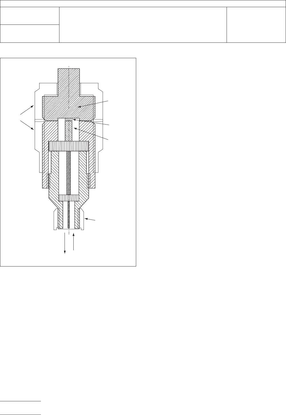
Test Fixture
The
test fixture consists of two Sections A
and B, where the specimen is placed in between, as shown in
Figure 1. The detailed drawings are given in Section 11. Sec-
tion A is an APC-7 to an APC-3.5 microwave adapter with
characteristic impedance of 50 Ω (Agilent 1250-1746). Sec-
tion B is an altered APC-7 short termination (Agilent 04191-
85300 or equivalent may be used), with a custom-machined
gap to accommodate a specimen of particular thickness.
When Sections A and B are assembled, the depth, d,ofthe
gap is equal to the specimen thickness. Specimens with dif-
ferent thickness will require separate Sections B. In the case
of a specimen thinner than 10 µm, the center conductor of the
APC-7 Section A may be replaced with a fixed 3.05 mm diam-
eter pin, machined precisely to achieve a flat and parallel con-
tact between the film specimen and the terminating Section B.
The diameter of the outer conductor, b, of Section A is
7.0 mm (see drawing in Section 11).
6
Measurement Procedure
6.1 Apparatus
The
measurement requires an automatic
vector network analyzer operating in the frequency range of
100 MHz to 18 GHz, for example an Agilent 8720D or equiva-
lent. The instrument should be equipped with a IEEE 488.2
I/O interface for transferring data between the network ana-
lyzer and a computing unit, e.g., a personal computer (PC)
with a General Purpose Input/Output Board (GPIB).
Connection between the test fixture (APC 3.5 adapter of Sec-
tion A) and the network analyzer shall be made using a phase
preserving coaxial cable, for example an Agilent 85131-60013
or equivalent.
6.2
Calibration Procedure
Set
the measurements range
to be between 100 MHz and 12 GHz. The number of data
points should be in the range of 800. The power level should
be set to 0 dBm with a dynamic range of at least - 40 dBm
(desirably to - 60 dBm ). Select the one Port S
11
measuring
mode
and Smith-Chart format. Connect the phase preserving
cable to the Port-1 of the network analyzer and to Section A
of the test fixture. Attach a calibration standard to Section A
of the test fixture. Perform an APC-7 Open, Load, Short cali-
bration using suitable calibration standards (Agilent 85050B
IPC-25510-1
Figure
1 Test fixture with a test specimen between
Sections A and B
SECTION B
APC-7
Mount
SECTION A
APC-3.5 Port
to Network Analyzer, S
11
Short
Standard
with a Gap
Test
Specimen
Center
Conductor
Pin
IPC-TM-650
Number
2.5.5.10
Subject
High
Frequency Testing to Determine Permittivity and Loss
Tangent of Embedded Passive Materials
Date
07/05
Revision
P
age2of8
电子技术应用 www.ChinaAET.com