IPC-TM-650 EN 2022 试验方法.pdf - 第411页
IPC-2-4-53-21 Figure 21 Example of Dye and Pull Location T ype Coverage Mapping B A = 0 % = 1 to 25 % = 26 to 50 % = 51 to 75 % = 76 to 100 % B C D E CD E 1 AX X X X B C D E F G H J K L M N O P Q R T U V W 23456789 1 0 1…
IPC-2-4-53-20
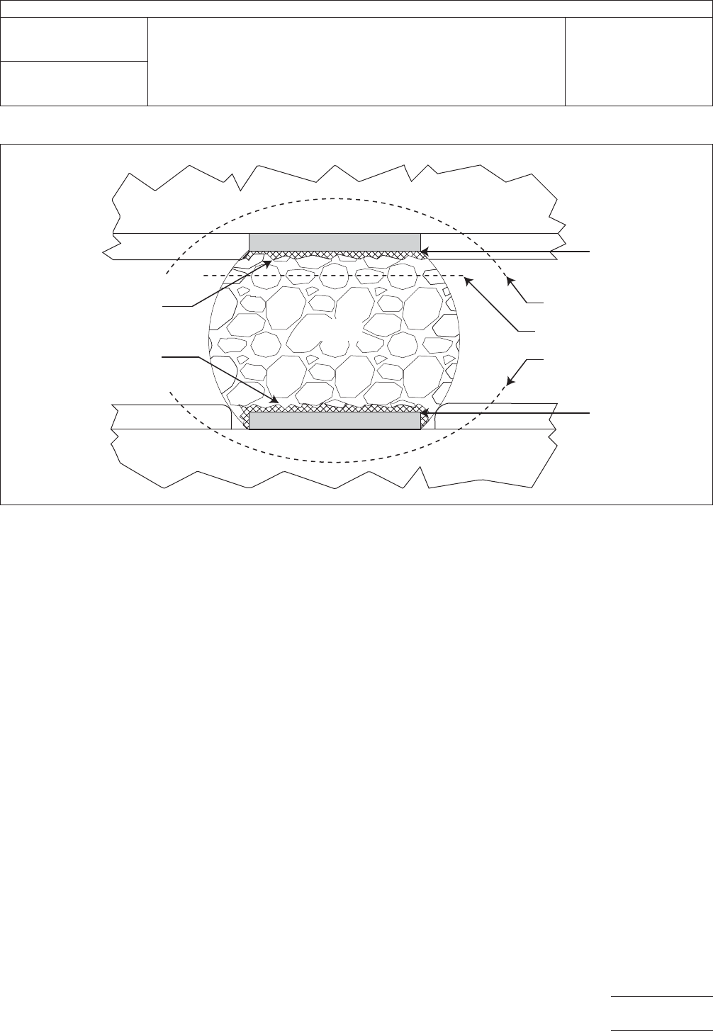
Figure 20 Typical Dye and Pull Separation Locations
A. Solder ball
B. Metal pad
C. Package substrate
D. Board
E. Fracture at package side intermetallic compound (IMC)/solder interface
F. Fracture at board side IMC/solder interface
G. Fracture at package metal/IMC interface
H. Package pad lift/crater
J. Fracture within bulk solder
K. Board pad lift/crater
L. Fracture at board metal/IMC interface
A
B
C
D
E
F
G
H
J
K
L
B
IPC-TM-650
Number
2.4.53
Subject
Dye and Pull Test Method (Formerly Known as Dye and Pry)
Date
8/2017
Revision
Page9of11
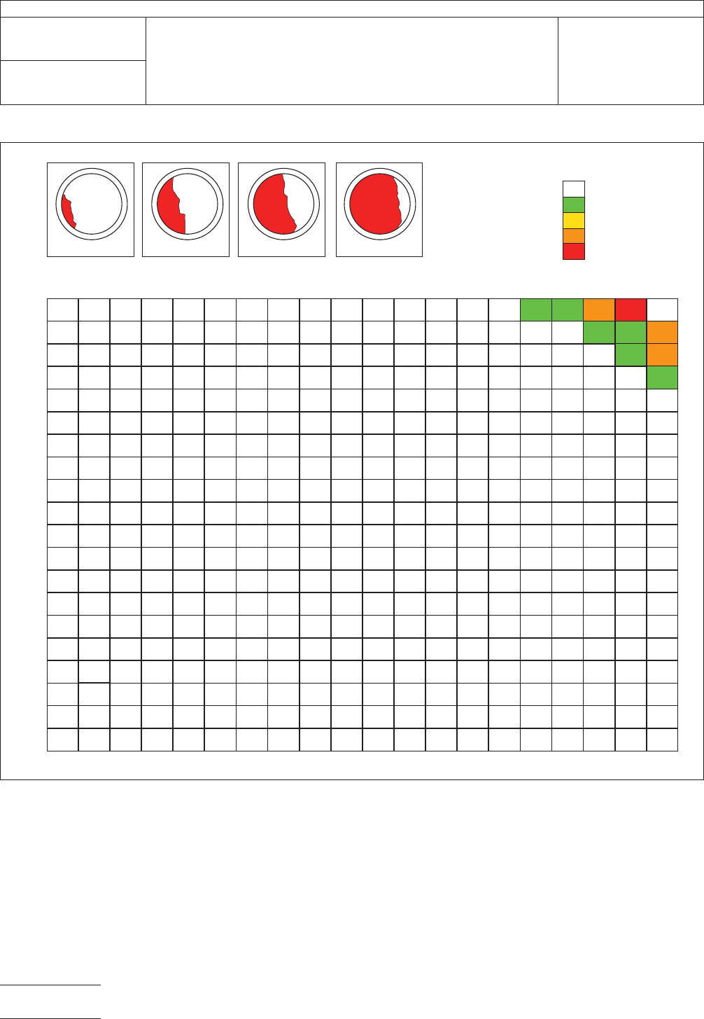
IPC-2-4-53-21
Figure 21 Example of Dye and Pull Location Type Coverage Mapping
B
A
= 0 %
= 1 to 25 %
= 26 to 50 %
= 51 to 75 %
= 76 to 100 %
B
C
D
E
CDE
1
AX
X X
X
B
C
D
E
F
G
H
J
K
L
M
N
O
P
Q
R
T
U
V
W
2345678910111213
2B 4B 3D
3D
2D
3E
3B
3B
2B
2B
14 15 16 17 18 19 20
IPC-TM-650
Number
2.4.53
Subject
Dye and Pull Test Method (Formerly Known as Dye and Pry)
Date
8/2017
Revision
Page 10 of 11
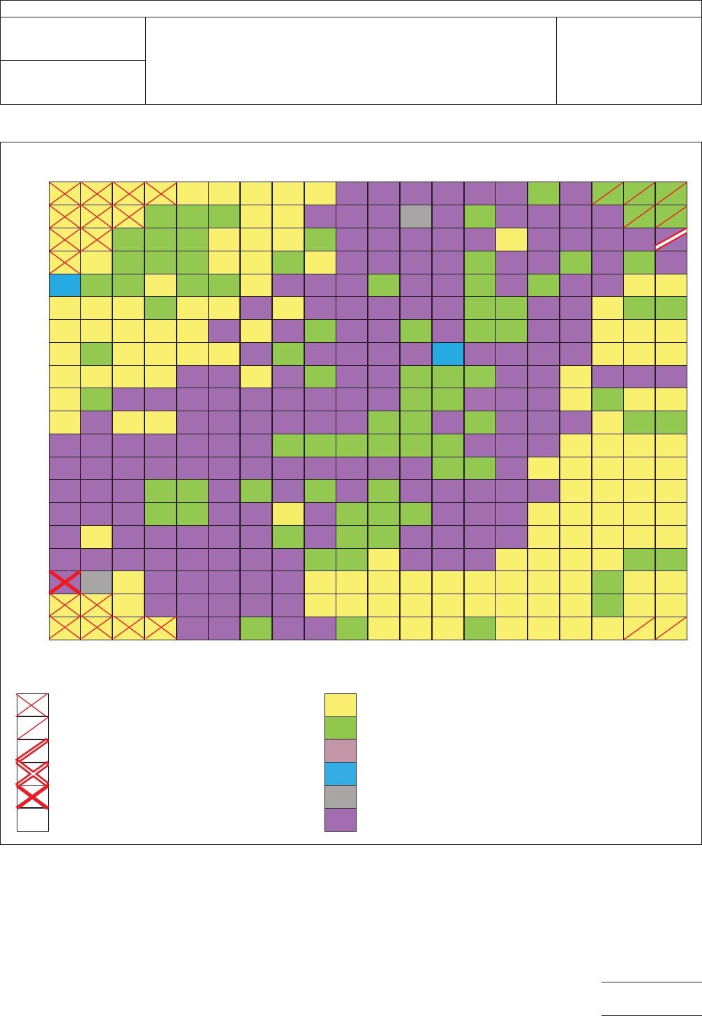
IPC-2-4-53-22
Figure 22 Second Example of Dye and Pull Location Type Coverage Mapping
a. Dye indication type
b. Separation mode
Note: The style of mapping in Figure 22 depicts every solder joint within the component by a color-coding system. Dye indications are then
additionally indicated by a red slash or “X” at each joint location as needed. Mapping components in this manner allows for quick evaluation of the
weakest interface of every solder joint and the location of any dye indications.
1
A
a
b
B
C
D
E
F
G
H
J
K
L
M
N
O
P
Q
R
T
U
V
W
2 3 45678 910111213 14 15 16 17 18 19 20
Complete dye indication
Partial dye indication
Partial dye indication at two interfaces
Complete dye indications at two interfaces
Partial and complete dye indication at two interfaces
No dye indication
Separation between board laminate and board pad
Separation between solder and board pad
Separation through solder joint
Separation between solder and component pad
Separation between component substrate and component pad
Other = Double separation between board laminate/board pad and
solder/board pad
IPC-TM-650
Number
2.4.53
Subject
Dye and Pull Test Method (Formerly Known as Dye and Pry)
Date
8/2017
Revision
Page 11 of 11