IPC-TM-650 EN 2022 试验方法.pdf - 第556页
frequencies where the conductor losses dominate. Addition- ally, in the high frequency range, the smoothing may preserve unrealistic features of the de-embedded insertion loss. 5.4.2 Cumulative Dielectric and Conductor L…
Probe performance may degrade over time. It is necessary to
periodically check the probe quality to assure the electrical
requirement in Figure 4-3 is met.
5 Procedure The procedure section is to be used to detail
all of the specific steps necessary to perform the actual test.
It shall include any specific conditioning requirements, or
other specimen preparation not previously detailed. It shall
then describe in detail the successive steps of the procedure,
grouping related operations into logical divisions in a concise
manner. It shall include times, temperatures, voltages, pres-
sures, concentrations, linear measurements and quantitative
criteria when necessary in applicable units (both Metric and
English).
It shall then state any detailed information required in report-
ing the test results. When two or more procedures are
described in the same test method, the report shall indicate
which of the procedures was used. When a test method
allows variations in operating or other conditions, the report
shall state the particular conditions utilized for the test.
This specification currently outlines measuring Frequency
Domain characteristics using a VNA.
5.1 VNA Settings Follow the VNA manual for proper
operation of equipment. Recommended settings for the VNA
include an IF bandwidth of 1 kHz (can be decreased based on
instrument and applications), and a step size of 10 MHz.
Smoothing is not allowed.
The cables and connectors used in the measurement should
be sufficiently rated for the maximum intended measurement
frequency.
5.2 Conditioning of Test Sample Refer to 3.8 for proper
conditioning of test sample before test.
5.3 VNA Calibration and De-embedding Calibration
and/or de-embedding techniques outlined in 1.2.1 must be
performed to remove the effects of cable, connector, and test
fixtures.
5.4 Smoothing and Fitting of Insertion Loss Measure-
ment Curve
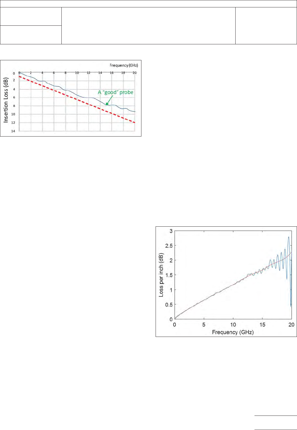
5.4.1 Insertion Loss Smoothing Basics
Printed board
testing facilities often report insertion loss per inch at a hand-
ful of frequencies (e.g., 4 GHz, 8 GHz, 12.89 GHz, etc.). An
ideal insertion loss curve for a printed board conductor is
expected to follow transmission line behavior and be smooth.
However, in some testing houses, the de-embedded insertion
loss curves may have oscillations and deviations due to vari-
ous sources of measurement and de-embedding error, as
shown in blue curve in Figure 5-1. Without proper post-
processing of the data, the measurement house can easily fail
to report the true loss performance of the test coupon at des-
ignated frequencies. One common methodology for obtaining
a smooth de-embedded insertion loss curve is to use an iter-
ated moving average. The result is a very smooth red curve
shown in Figure 5-1.
While smoothing with an iterative moving average addresses
most of the challenges posed by the measurement errors,
there remain some disadvantages. The resulting smooth curve
is non-physical and unlikely to be representative of the true
loss of printed board conductor. For example, the smoothed
curve usually deviates from the correct answer at low
IPC-25514-4-3
Figure 4-3 Insertion Loss Requirement for the Probe
Quality Test Setup in Figure 4-2
IPC-25514-5-1
Figure 5-1 An Iterative Moving Average Applied to a
Typical Insertion Loss Curve
Note 1. Red denotes the smoothed curve
IPC-TM-650
Number
2.5.5.14
Subject
Measuring High Frequency Signal Loss and Propagation on
Printed Boards with Frequency Domain Methods
Date
02/2021
Revision
Page7of11
frequencies where the conductor losses dominate. Addition-
ally, in the high frequency range, the smoothing may preserve
unrealistic features of the de-embedded insertion loss.
5.4.2 Cumulative Dielectric and Conductor Loss Fit-
ting
As it has been discussed in [14], the cumulative dielec-
tric and conductor losses can be generally approximated by
IL
dB
(,) = a
√
, + b, + c,
2
(Eq. 6)
where , is the frequency in GHz and a, b and c are constants.
For most of the cases coefficient c << 1 and can be
neglected. Therefore, as a first approximation the total loss
curve can be fitted to
IL
dB
(,) = a
√
, + b, (Eq. 7)
There are number of algorithms that can be used to perform
the printed board loss fit to Eq. 7. One of the most well-known
and widely available algorithms is the least squares fit,
example of which is shown in the Figure 5-2 below.
Even though least squares generally provide a good curve
approximation with the specified behavioral function, there are
many other fitting algorithms that can be applied.
5.4.3 An Alternative Cumulative Dielectric and Conduc-
tor Loss Fitting
Alternatively, when losses cannot be fitted
to the conventional physical based behavioral functions in (Eq.
6) and (Eq. 7), especially when measurement raw data has
high ringing resonances, other empirical approximations can
be used. Fox example, in [15], the following function is set as
the target function for the fitting algorithm:
IL
dB
(,) = a(, – ,
0
)
b
+c(, – ,
0
)
2
+ d(, – ,
0
) + IL
0
(Eq. 8)
The first term represents the AC conductor loss (i.e., the skin-
effect losses), where ‘b’ is an additional fitting parameter
(instead of a constant 0.5 where ideal conductor loss is a
function of ,
0.5
) added to take into account the surface rough-
ness impact of the conductor. The second and the third terms
represent dielectric losses, and the constant represents the
conductor’s DC loss. Furthermore, a certain offset point (,
0
,
IL
0
) is introduced, where ,
0
is the first frequency point of the
measurement. The offset is added to accommodate the fact
that VNA measurements made at the printed board fabricator
usually do not provide results lower than 10 MHz.
The abovementioned methods fit the data to a smooth curve
over the entire bandwidth of the measurement where each
data point is allocated equal weight. As measurement errors
usually increase significantly at high frequencies, a weighting
scheme can be introduced to force the algorithm to prioritize
the curve fitting at the low frequencies and minimize (or ignore)
the impact of high frequency:
W(,) =
(
1–
(
,
,
max
))
3
(Eq.9)
where ,
max
is the maximum measurement frequency. Figure
5-3 shows the suggested weighted function where ,
max
=20
GHz.
IPC-25514-5-2
Figure 5-2 Least Squares Fit Based on (eq. 7) Applied to
a Representative Insertion Loss Curve
Note 1. Red represents the fitted curve.
IPC-25514-5-3
Figure 5-3 The Suggested Weight Function for Insertion
Loss Curve Fitting
IPC-TM-650
Number
2.5.5.14
Subject
Measuring High Frequency Signal Loss and Propagation on
Printed Boards with Frequency Domain Methods
Date
02/2021
Revision
Page8of11
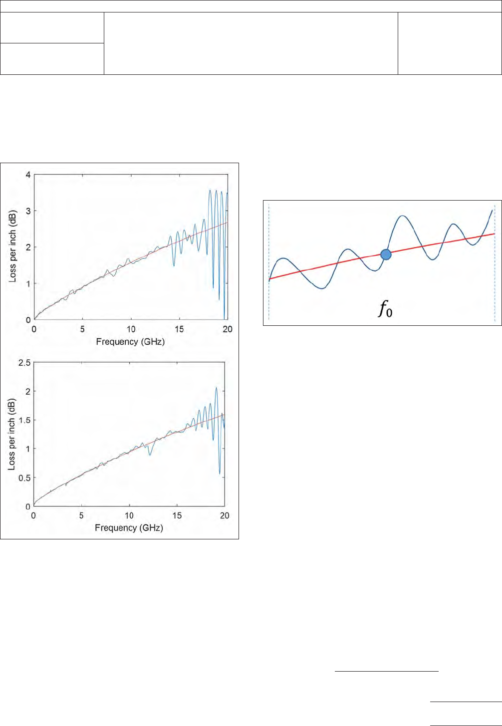
Typical least mean square fit approach is applied to fit the
weighted raw data to the target function. Figure 5-4 shows
the fitted insertion loss curve for two measurement cases
using the procedures described above.
5.4.4 Addressing the Quality of Reported Insertion
Loss
As mentioned previously, when performing measure-
ments on printed board conductors to check whether they
pass insertion loss requirements, printed board testing houses
generally only provide the insertion loss at a few points in their
report. Usually, the reported loss value using the fitted value
provides results with better fidelity compared to the raw data.
Meanwhile, the deviation of the reported values from the raw
data is a good indicator on the quality of the measurement.
The simplest approach to compute the uncertainty at the
selected frequency is to use the difference between the raw
data and fitted results. However, this can be misleading,
which is demonstrated in Figure 5-5. In this case, the devia-
tion of raw data from the fitted curve is zero at the selected
frequency, while it is clear that the measurement quality is not
perfect.
To quantify the uncertainty of the reported insertion loss at the
point of interest it is necessary to analyze the fit deviation in its
immediate vicinity, as shown in Figure 5-5. An ‘error neighbor-
hood’ of±1GHz(can be adjust based on user’s specific
application) is suggested to calculate the fit precision using
the distribution of the residuals within the±1GHzfrequency
range. For frequency points at the lower or upper limit of the
measurement bandwidth, the ± 1 GHz bound can be adjusted
so that the ‘neighborhood error bound’ does not extend
beyond the measurement bandwidth. For example, if the
measurement upper frequency limit is 20 GHz, and the fre-
quency of interest is 19.5 GHz, then the ‘neighborhood error
bound’ is from 18.5 to 20 GHz.
From the fitted curve and the original raw data, the residuals,
ILres(i) are calculated for all the frequency points within the ±
1 GHz range:
IL_res( i )=IL_raw( i )–IL_fit( i ) (Eq. 10)
where IL_raw(i) is the raw data of insertion loss at each fre-
quency points, and IL_fit(i) is the fitted insertion loss. The
mean and standard deviation (σ) of the residual distribution is
calculated, and the uncertainty at given frequency f0 is
defined as:
uncertainty@,
0
=
mean (IL
_res
) +3xσ(IL
_res
)
IL
_fit
@,
0
x 100% (Eq.11)
IPC-25514-5-4
Figure 5-4 Examples of an Alternative Insertion Loss
Fitting using Eq. 6
IPC-25514-5-3
Figure 5-5 Deviation of the Raw Data from the Fitted
Curve at a Single Frequency Point can be Misleading
IPC-TM-650
Number
2.5.5.14
Subject
Measuring High Frequency Signal Loss and Propagation on
Printed Boards with Frequency Domain Methods
Date
02/2021
Revision
Page9of11