IPC-TM-650 EN 2022 试验方法.pdf - 第361页
CHECKLIST 1. Is the specimen size 300 mm x 280 mm [12 in x 11 in]? ......................................................... ____ 2. Is the warp direction properly identified? ................. ____ 3. Were the four loca…

5.2
Copper Removal
Remove
copper by etching in cupric
chloride containing spray etcher at less than 50°C (122°F).
Rack samples upon exit from etcher, rinse, remove the tape,
and air-dry laminate. Submit to bake cycle (paragraph 5.3)
within four hours. (
Note:
Do
not use resist stripping solutions.)
5.3 If only the thermal stress cycle is to be used proceed to
5.5. If not, proceed to 5.4.
5.4
Bake Cycle
5.4.1
Bake
specimens at 105°C ± 5°C for four hours ± 10
minutes. Vertically rack and place specimens in oven parallel
to air flow with specimens being separated by a minimum of
1/2 inch.
5.4.2
After
baking, immediately place the test specimens in
a stabilization chamber (paragraph 4.3).
5.4.3
Remove
from stabilization chamber after one hour
+
1
⁄
2
/-0
hours and, within 5 minutes, measure W1
1
,W
2
1
,F
1
1
,
and
F2
1
,
using the apparatus defined in paragraph 4.1.
5.4.4
If
the thermal stress cycle is to be included in this test,
proceed to paragraph 5.5. If not, proceed to 5.6.
5.5
Thermal Stress Cycle
After
the bake cycle measure-
ment (5.4), if immediate further processing is not feasible,
place specimens in a stabilization chamber until test is contin-
ued.
5.5.1
If
a stabilization chamber is used, remove from the
stabilization chamber and bake specimens at 150°C ± 5°C for
two hours ± 5 minutes. Vertically rack and place specimens in
oven parallel to air flow, with specimens being separated by a
minimum of 1/2 in.
5.5.2
After
baking, immediately place the test specimen in a
stabilization chamber (paragraph 4.3).
5.5.3
Remove
from stabilization chamber after 1 hour + 1/ 2
hour, -0 hours, and, within 5 minutes, measure W1, W2, F1,
and F2, using the apparatus indicated in paragraph 4.1.
Record values as W1
2
,W
2
2
,F
1
2
,
and F2
2
.
5.6
Evaluation
Determine
the change in dimensional sta-
bility using the following formulation:
5.6.1
Warp Evaluations
Warp =
W1
1
− W1
W1
x1
0
3
= Mils/per
inch for W1 after bake
W2
1
− W2
W2
x1
0
3
= Mils/per
inch for W2 after bake
Repeat for W1
2
and
W2
2
for
after stress
Where W1/W2 = initial dimensions,
W1
1
/W2
1
=
after bake dimensions, and
W1
2
/W2
2
=
after thermal stress.
5.6.2
Fill Evaluations
Fill =
F1
1
− F1
F1
x1
0
3
= Mils/per
inch for F1 after bake
F2
1
− F2
F2
x1
0
3
= Mils/per inch for F2 after bake
Repeat for F1
2
and
F2
2
for
after stress
Where F1/F2 = initial dimensions,
F1
1
/F2
1
=
after bake dimensions, and
F1
2
/F2
2
=
after thermal stress.
5.6.3
Calculations
Take
the warp dimensions made on all
the measured specimens and determine the mean value for
the warp dimensional stability characteristics of the laminate
after bake. Follow similar procedures on the calculations for
the fill dimensional stability characteristics after bake. Extreme
values should be eliminated using the procedure defined in
paragraph 5.6.4. Similar measurements are made to calculate
the after thermal stress dimensional stability characteristics.
5.6.4
Extreme Value Eliminated
Take
measurements in
subgroup (warp or fill) and arrange in descending order of
magnitude. Solve for D, using procedure detailed in Table 1. If
calculated D is larger than the value of D shown in Table 2 for
the number of measurements being evaluated, the outlier is
significant and should be deleted.
6.0 Notes
The following is a checklist that should be used
by personnel responsible for performing this method in order
to provide repeatable/correlatable results. The IPC Dimen-
sional Stability Task Group responsible for the technical report
on dimensional stability has determined that checklist items 2,
5, 6, 9, 14, 15, 16 and 18 are critical to appropriate use of this
procedure. (See IPC-TR-463.)
IPC-TM-650
Number
2.4.39
Subject
Dimensional
Stability, Glass Reinforced Thin Laminates
Date
2/86
Revision
A
P
age2of3
电子技术应用 www.ChinaAET.com
CHECKLIST
1. Is the specimen size 300 mm x 280 mm
[12 in x 11 in]?......................................................... ____
2. Is the warp direction properly identified? ................. ____
3. Were the four location points prepared by either
drilling or scribing?................................................... ____
4. Were the measured points located approximately
12 mm [0.5 in] from each edge of the fill direction
and approximately 25 mm [1.0 in] from each edge
of the warp direction?.............................................. ____
5. Were the measurements taken from the same
feature location, i.e., edge of the hole, center,
scribe mark, etc?..................................................... ____
6. Were specimens processed without mechanical
or chemical pre-cleaning?........................................ ____
7. Was cupric chloride etching with spray used to
remove the copper? ................................................ ____
8. Was the temperature of the etching less than
50°C? ...................................................................... ____
9. The specimens were not exposed to resist
stripping solution?.................................................... ____
10. Were specimens racked after removal from
etching cycle?.......................................................... ____
11. Is the oven used for baking capable of ± 2°C
control and has a recovery time of less than
15 minutes?............................................................. ____
12. Were specimens subjected to the bake cycle
within 4 hours after etching?.................................... ____
13. Were the specimens baked at 105°C ± 5°C for
4 hours and vertically racked? ................................. ____
14. Was the stabilization chamber capable of
maintaining 20% RH maximum at 21 ± 2°C? .......... ____
15. Was each specimen removed from stabilization
after 1 hour + 1/2 hour -0 hours and were all
measurements taken within 5 minutes?................... ____
16. Were samples stored in stabilization chamber
between after bake and after thermal stress
measurements if immediate processing not
feasible?................................................................... ____
17. Were specimens thermal stressed at 150°C
± 5°C for two hours and vertically racked?.............. ____
18. Was each specimen removed from stabilization
after 1 hour + 1/2 hour -0 hours and were all
measurements taken within 5 minutes?................... ____
Note:
When
using the above checklist, all answers should be
affirmative. The technician performing the test should sign the
report, record the date and times of all actions taken, and
report any deviations on the procedure.
T
able 1 Calculation Procedure
Subgroup
Size
If
Apparent Outlier
is Largest Value
If Apparent Outlier
is Smallest Value
n
= 3-7
D =
Largest Value −
2nd Largest Value
Largest
Value −
Smallest Value
D =
2nd Smallest Value −
Smallest Value
Largest
Value −
Smallest Value
n = 8-10
D =
Largest Value −
2nd Largest Value
Largest
Value −
2nd Smallest Value
D =
2nd Smallest Value −
Smallest Value
2nd
Largest Value −
Smallest Value
Table 2 Extreme Value Table
n
D (Confidence Level 95%)
3
0.941
4 0.765
5 0.642
6 0.560
7 0.507
8 0.554
9 0.512
10 0.433
IPC-TM-650
Number
2.4.39
Subject
Dimensional
Stability, Glass Reinforced Thin Laminates
Date
2/86
Revision
A
P
age3of3
电子技术应用 www.ChinaAET.com
1
Scope
This
method is used to determine the inner layer
bond strength of either a metal conductor or an individual
dielectric.
2
Applicable Documents
None
3
Test Specimen
Laminate
dielectric with or without cop-
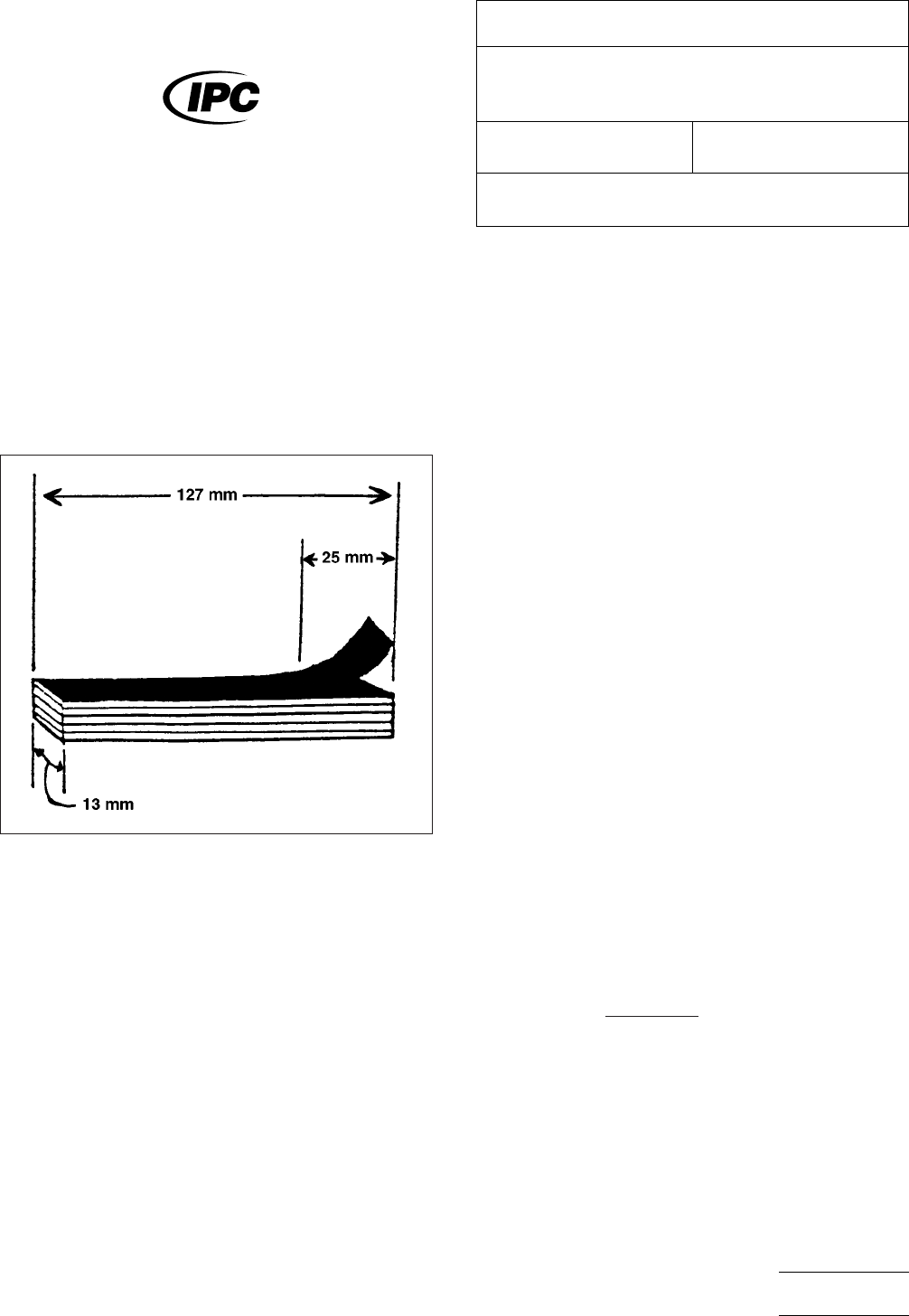
per foil, prepared in accordance with Figure 1.
4
Equipment/Apparatus
4.1
Unite-O-Matic
tensile tester Model #FM 10 or equivalent
4.2
Scalpel
5
Procedure
5.1 Preparation for Testing
During
layup of the test
specimen panel, place ‘‘TEDLAR’’ (or other suitable material)
release sheets that will disallow lamination at one end of each
specimen, providing a 13 mm x 25 mm non-bonded tab. The
tabs can then be used as gripping areas to perform bond
strength testing. One can then evaluate the laminate-to-
laminate bonds and the laminate-to-copper foil bond through-
out the finished panel thickness.
5.1.1
Place
an equal number of release sheets on the outer
surface of the layup, covering all surfaces, except where inter-
nal release sheets have been placed. This is essential to pro-
vide proper and uniform lamination pressure.
5.1.2
After
lamination and cure, cut the panel into 25 mm
strips, as shown in Figure 1, and remove internal release
sheets.
5.1.3
If
steps 5.1.1 and 5.1.2 are not used, it will be neces-
sary to chemically or thermally remove resins from the outer
25 mm, in order to provide a tab to initiate testing.
5.2
After
cutting the samples to the designated size and lift-
ing the 25 mm strip for testing, the layer to be tested shall be
fastened into the clamping device of the tensile tester, allow-
ing the wire connecting the clamp to the tensile tester to pull
the specimen vertically within ± 5° angle.
5.3
The
tester is then started. A force is applied in the verti-
cal direction at a rate of 51 mm per minute until delamination
(bond strength) is completed or the inner layer tears.
The minimum load is then recorded using the following for-
mula:
Bond strength of the conductor width =
25mm
sample
width
x total load
IPC-2-4-40-1
Figure
1 Laminate Dielectric
The
Institute for Interconnecting and Packaging Electronic Circuits
2215 Sanders Road • Northbrook, IL 60062-6135
IPC-TM-650
TEST
METHODS MANUAL
Number
2.4.40
Subject
Inner
Layer Bond Strength of Multilayer Printed
Circuit Boards
Date
10/87
Revision
Originating Task Group
N/A
Material
in this Test Methods Manual was voluntarily established by Technical Committees of the IPC. This material is advisory only
and its use or adaptation is entirely voluntary. IPC disclaims all liability of any kind as to the use, application, or adaptation of this
material. Users are also wholly responsible for protecting themselves against all claims or liabilities for patent infringement.
Equipment referenced is for the convenience of the user and does not imply endorsement by the IPC.
P
age1of1
电子技术应用 www.ChinaAET.com