IPC-TM-650 EN 2022 试验方法.pdf - 第603页
3.1 Conductor Any high resistance conductor used in HDI applications (polymer thick film, via fill, metal, metal compos- ites, transient liquid phase sintering, organometallic, conduc- tive polymer, etc.). Copper foils u…
1
Scope
This
test method covers the two-wire resistance
test for the determination of the volume resistivity of polymer-
based conductive pastes and other conductive materials used
in HDI. This test is valid for conductive materials with volume
resistivity on the order of 10
-5
Ω-cm
or higher. For measuring
resistivity on highly conductive materials or any material that
cannot be patterned into a circuit pattern, a four-wire (Kelvin
Probe) test method, such as IPC-TM-650, Method 2.5.14, is
recommended.
1.1
Definition
Volume
resistivity is a material property that
can be utilized to calculate the resistance in a circuit design.
For materials with high resistivity, a two-wire resistance test
may be used to measure the volume resistivity.
The resistance in any sample (R in units of Ω) is related to the
dimensions of the test circuit and the volume resistivity (ρ)
inherent in the material (see Figure 1).
R =ρ
(
L
tW
)
L,
W, and t are the length, width, and thickness respectively
of the test circuit (in cm). The quantity L/W is called a square,
([). The volume resistivity can then be expressed as:
ρ=
Rt
(
L
W
)
=
Rt
[
with
units of ohms-cm (Ω-cm).
2
Applicable Documents
IPC-TM-650
Test
Methods Manual
2.5.14 Resistivity of Copper Foil
3
Test Specimen
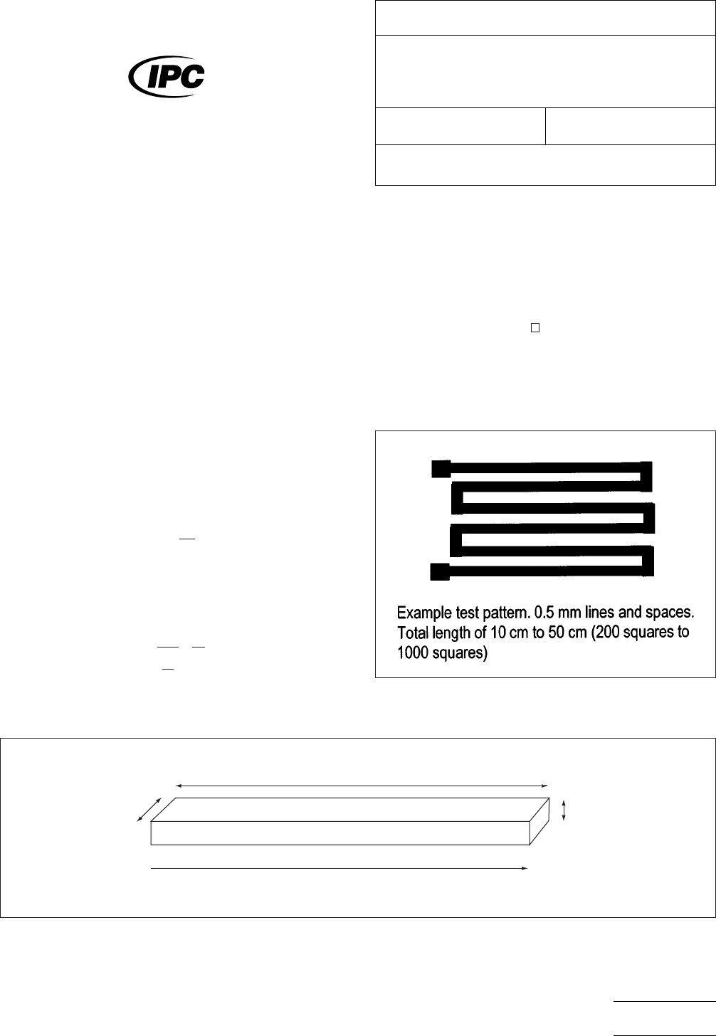
The
test specimen is a 0.5 mm wide
serpentine circuit pattern (see Figure 2) with a length of
between 200 [ and 1000
(length
equal to 200 to 1000
times the width) prepared by screen printing or other meth-
ods. Specimens may be prepared by other methods, as long
as they have measurable dimensions. If materials cannot be
prepared in a circuit pattern, see 6.2.
IPC-2-5-17-2-1
Figure
1 Resistivity Diagram
Conductor
Length = L
Current Flo
w
Width = W
Thickness = t
IPC-25172-2
Figure
2 Serpentine Pattern
The
Institute for Interconnecting and Packaging Electronic Circuits
2215 Sanders Road • Northbrook, IL 60062
IPC-TM-650
TEST
METHODS MANUAL
Number
2.5.17.2
Subject
Volume
Resistivity of Conductive Materials Used in
High Density Interconnection (HDI) and Microvias,
Two-Wire Method
Date
11/98
Revision
Originating Task Group
HDI Test Methods Task Group (D-42a)
Material
in this Test Methods Manual was voluntarily established by Technical Committees of the IPC. This material is advisory only
and its use or adaptation is entirely voluntary. IPC disclaims all liability of any kind as to the use, application, or adaptation of this
material. Users are also wholly responsible for protecting themselves against all claims or liabilities for patent infringement.
Equipment referenced is for the convenience of the user and does not imply endorsement by the IPC.
P
age1of3
电子技术应用 www.ChinaAET.com

3.1
Conductor
Any
high resistance conductor used in HDI
applications (polymer thick film, via fill, metal, metal compos-
ites, transient liquid phase sintering, organometallic, conduc-
tive polymer, etc.). Copper foils used in HDI should be tested
according to IPC-TM-650, Method 2.5.14.
3.2
Substrate
Unless
otherwise specified, the substrate
shall be a PCB laminate, etched to remove all copper. Other
acceptable substrates (when specified) may be plate glass,
insulated metals, or flexible circuit base material.
3.3
Screen
For
materials that are screen printed, unless
otherwise specified, the screen shall be as outlined in 3.3.1
through 3.3.3.
3.3.1
Type
200
mesh, stainless steel, 35 µm wire
3.3.2
Emulsion
<15
µm emulsion build up
3.3.3
Wire Angle
22.5°
to 45°
3.4
Typical Patterns
3.4.1 Pattern
Serpentine
with 0.5 mm wide lines and
spaces and 200 [ to 1000 [ long (10 cm to 50 cm). The
larger the number of squares, the higher the resistance and
more accurate the measurement.
3.4.2
Print
1.25
mm snapoff
0.2 Kg to 1.0 Kg squeegee pressure per cm squeegee length
2.5 cm/sec. to 12.5 cm/sec. draw speed
3.5
Cure Conditions
The
conductor shall be cured
according to the manufacturer’s specifications. Parts are
allowed to cool to room temperature, after which they are
measured for resistance.
4
Equipment/Apparatus
4.1
A
digital multimeter capable of resolving 0.1 Ω resis-
tance is required. This unit must be accurately calibrated. An
example would be a Fluke 70 series digital multimeter. For
improved accuracy in this measurement, a larger number of [
and/or a more sensitive multimeter can be utilized.
4.2
A
screen printer capable of making 0.5 mm line/space
circuitry, or any other method for preparing the desired circuit
pattern
4.3
Equipment
to measure the test circuit conductor length,
width, and thickness. If the number of squares is accurately
known (length/width of circuit) from the artwork and standard
process conditions, then only the thickness needs to be mea-
sured on each specimen. Thickness can be determined by
various methods: cross-section/optical microscopy, profilo-
meter measurement, or calculation from deposition weight
and material density. If the circuit thickness is very uniform,
then optical sectioning is the preferred method for obtaining
the thickness. If the circuit thickness is thought to be non-
uniform, thickness may then be determined by averaging pro-
filometer readings or determining average thickness from the
weight of the material deposited (knowing the length, width,
and density that the thickness can be determined).
5
Procedure
5.1 Samples
Prepare
a minimum of five test specimens
according to 3.1 through 3.5.
5.2
Conditioning
Condition
the specimens at 23°C ± 5°C,
50% RH (± 5%) for 24 hours.
5.3
Measurement
5.3.1
Measure
the circuit length, width, and thickness using
the equipment described in 4.3.
5.3.2
Apply the digital multimeter leads to the pads at each
end of the circuit. Measure and record the resistance in ohms.
For a resistance less than 2 Ω, see 6.1.
5.3.3
Measure
the resistance of a minimum of five speci-
mens and average the values.
5.4
Calculation
Calculate
the volume resistivity for each
specimen from the equation below:
ρ
i
=
Rt
(
L
W
)
where:
R
= average resistance of a single specimen in ohms
t = thickness of the conductive specimen in cm
L = length conductive specimen in cm
W = width conductive specimen in cm
Note: The ratio L/W is the number of squares.
IPC-TM-650
Number
2.5.17.2
Subject
Volume
Resistivity of Conductive Materials Used in High Density
Interconnection (HDI) and Microvias, Two-Wire Method
Date
11/98
Revision
P
age2of3
电子技术应用 www.ChinaAET.com

Calculate
the average resistivity from the sum of the specimen
volume resistivities:
ρ
ave
=
Σ
ρi
n
n
where:
n
= number of specimens measured
Note: The units of resistivity are Ω-cm.
5.7
Report
5.7.1
Report
the volume resistivity in units of Ω-cm.
5.7.2
Report
the substrate used in the test.
5.7.3
Report
the test circuit length, width (or squares), and
thickness.
6 Notes
6.1
Low Resistance Measurements
For
test circuits with
a resistance less than 2.0 Ω, the contact resistance between
the probe and the pads will be significantly relative to the
resistance arising from the test circuit. The 2.0 ohm lower
limit, in combination with the 0.1 ohm sensitivity of the multi-
meter, provides for a minimum error of 5%.
One solution is to increase the length of the circuit (increase
the number of squares) to increase the resistance. Another
solution for measuring resistivity on a highly conductive mate-
rial is to change to a four-wire (Kelvin Probe) test method,
such as IPC-TM-650, Method 2.5.14.
6.2
Test Circuit Specimens
It
is anticipated that some
materials cannot be formed into a uniform test circuit, as
called out for in this test method. It is recommended that
these materials be tested with a four-wire method (IPC-TM-
650, Method 2.5.14) and an alternative construction.
For example, a thin film of conductive material (i.e., paste or
conductive film) can be placed between two metal plates and
the resistivity may be determined using the four-wire (Kelvin
Probe) method. The material thickness and contact area must
be known, and the material must be sufficiently compliant to
completely wet (contact) the two plates.
6.3
Other References
Gilleo,
Ken, Polymer Thick Films, Van Nostrand Reinhold,
1996
IPC-TM-650
Number
2.5.17.2
Subject
Volume
Resistivity of Conductive Materials Used in High Density
Interconnection (HDI) and Microvias, Two-Wire Method
Date
11/98
Revision
P
age3of3
电子技术应用 www.ChinaAET.com