IPC-TM-650 EN 2022 试验方法.pdf - 第308页
1 Scope This test method is used to determine the resis- tance of laminate materials (both unclad and etched surfaces) to the thermal abuse of a solder dip. Resistance to softening, loss of surface resin, scorching, dela…
5.7.1
Calculate
the average effective radius of curvature and
the standard deviation for each wafer from the 4 measure-
ments made on each wafer in step 5.3.2 using the following
equation:
R =
(R
1
R
2
)
(R
1
− R
2
)
where
R1 and R2 are the radius of curvature of the uncoated
and coated wafers respectively. The standard deviation is cal-
culated as follows and reported to two significant figures:
S
x
=
√
N
Σ
N
i = 1
X
i
2
−
(
Σ
N
i = 1
X
i
)
2
N(N−1)
where
X
i
is
the value of a single observation (i = 1 through N),
N is the number of observations and s
x
is
the estimated stan-
dard deviation.
5.7.3
Calculate
the average effective radius of curvature for
each film thickness using the averages from step 5.7.1 of all
three wafers at the same film thickness. Do not include in the
calculation the data from any wafer for which the standard
deviation from 5.7.1 is greater than 10%.
5.7.4
Convert
the average effective radius of curvature for
each film thickness from step 5.7.3 into the wafer deforma-
tion, h, using the following equation
h = R
A
−
√
R
A
2
−
L
2
4
where
L is the diameter of the wafer and R
A
is
the average
effective radius of curvature obtained in 5.7.3.
5.7.5
Curvature Slope
The
wafer deformation values for
each film thickness from step 5.7.4 are plotted as wafer defor-
mation (y-axis) versus film thickness (x-axis). An equation of
theformy=mx(i.e. a straight line with intercept atx=0,y=
0) is fit to the data (unweighted) and the slope of the line can
be used to compare different materials or processes when
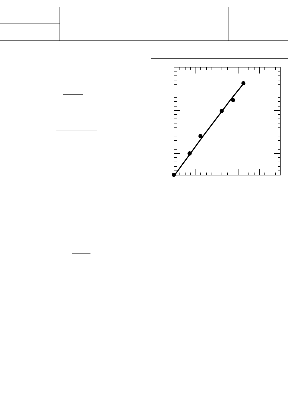
coated on identical substrates. A typical plot is illustrated in
Figure 1.
6.0 Notes
6.1
The
Flexus determines the radius of curvature by shining
a He-Ne laser beam through a beam splitter. The two beams
are reflected off the surface of the wafer into detectors. The
radius of curvature, R, is calculated from the angle of reflec-
tion and the distance between the two beams. If measure-
ments are made on the coated side of the wafer, the laser
beam is refracted twice, once upon entering the polymer layer
and again upon exiting the polymer layer. As the polymer layer
increases in thickness, the refracted laser beam can no longer
be correctly detected by the detector, resulting in erroneous
values for the radius of curvature. In practice, the upper limit
on thickness for polyimides was found to be approximately
10-12 µm. To avoid this complication, the polymer films are
deposited on the back of the wafers and the measurements
are made on the front (polished side) of the wafer. This
extends the useful thickness range to 50 µm.
6.2
The
radius of curvature will depend on the thickness of
the wafer. Wafers of comparable thickness (625 ± 15 µm)
must be used when making comparisons of different
materials.
2.4.22.2−01
Figure
1
Film Thickness (µm)
Curvature
Slope = 3.3
Wafer Deformation (
µ
m)
50
40
30
20
10
0
048
121620
IPC-TM-650
Number
2.4.22.2
Subject
Substrate
Curvature: Silicon Wafers with Deposited Dielectrics
Date
7/95
Revision
P
age2of2
电子技术应用 www.ChinaAET.com

1
Scope
This
test method is used to determine the resis-
tance of laminate materials (both unclad and etched surfaces)
to the thermal abuse of a solder dip. Resistance to softening,
loss of surface resin, scorching, delamination, blistering and
measling are considered in the evaluation.
2
Applicable Documents
IPC-TM-650
Test
Methods Manual
2.4.1 Adhesion, Tape Testing
2.4.12 Solderability, Edge Dip Method
MIL-F-14256
Flux
3
Test Specimen
Each
specimen must be 3.18 cm x 3.18
cm thickness. A separate specimen is required for the unclad,
etched, fluxed, and unfluxed tests. Three samples are
required from each sheet.
4
Equipment/Apparatus
4.1
An
electrically heated, thermostatically controlled pot of
sufficient size to accommodate the specimen and containing
no less than 2.25 kg of Sn6O or Sn63
4.2
A
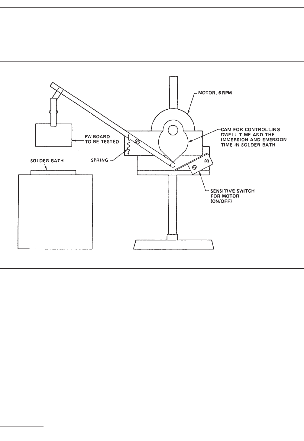
device, as shown in Figure 1, or some other similar
device may be used, if:
• The rate of immersion, dwell time, and withdrawal are within
the test limits described in the procedure
• The specimen and solder surface remain perpendicular
within 5°
• Wobble, vibrations, and other extraneous movements are
eliminated
4.3
Warnow
2-710 black acid resisting ink, or equivalent
4.4
NAZ-DAR
ER-111 black epoxy ink, or equivalent
4.5
A
convection drying oven capable of attaining at least
149°C
5
Procedure
5.1 Etched and Unetched Specimen
5.1.1
Expose:
•
One specimen having a surface upon which no metal clad-
ding was ever applied
• One specimen on which the metal cladding has been
removed by standard etching processes
• One specimen with metal cladding remaining to the Solder-
ability Edge Dip Method in IPC-TM-650, Method 2.4.12
5.1.2
Examine
the specimens for evidence of discoloration
or surface contaminants, loss of surface resin, softness,
delamination, interlaminar blistering, or measles. The speci-
men having metal cladding must also be examined for blister-
ing or delamination of the metal foil from the laminate material.
5.2
Plastic Surface Tape Test
5.2.1
Screen
print one of the test inks to the surfaces of an
unclad specimen and an etched specimen.
5.2.2
Treat
test inks as follows:
1. Warnow 2-710: Cure for a minimum of 30 minutes in air or
oven. The dry film must be hard and dull in finish.
2. NAZ-DAR ER-111: Cure for a minimum of 8 minutes at
135°C. The cured ink must have a hard glossy finish.
5.2.3
After
the specimens have cured properly, perform the
plating adhesion test on the inked surfaces, as defined in IPC-
TM-650, Method 2.4.1. Use type I class A tape.
5.2.4
Carefully
examine specimens for the items discussed
in 5.1.2.
5.2.5
Examine
for evidence of mold release agents, indi-
cated by particles of ink adhering to the tape, or by the
absence of ink from the laminate surface, or both.
5.3
Fluxed and Unfluxed Specimens
The
Institute for Interconnecting and Packaging Electronic Circuits
2215 Sanders Road • Northbrook, IL 60062-6135
IPC-TM-650
TEST
METHODS MANUAL
Number
2.4.23
Subject
Soldering
Resistance of Laminate Materials
Date
3/79
Revision
Originating Task Group
N/A
Material
in this Test Methods Manual was voluntarily established by Technical Committees of the IPC. This material is advisory only
and its use or adaptation is entirely voluntary. IPC disclaims all liability of any kind as to the use, application, or adaptation of this
material. Users are also wholly responsible for protecting themselves against all claims or liabilities for patent infringement.
Equipment referenced is for the convenience of the user and does not imply endorsement by the IPC.
P
age1of2
电子技术应用 www.ChinaAET.com
5.3.1
Clean
the metal clad specimen by light abrasion or
other suitable method, then flux the metal surface with a rosin
flux conforming to MIL-F-14256.
5.3.2
Clean
the unclad specimens by standard production
techniques, then flux the laminate material with a rosin flux
conforming to MIL-F-14256.
5.3.3
Carefully
examine all specimens, then perform the
tests described in 5.1.1 through 5.2.5.
IPC-2412-1
Figure
1 Suggested Dipping Device
IPC-TM-650
Number
2.4.23
Subject
Soldering
Resistance of Laminate Materials
Date
3/79
Revision
P
age2of2
电子技术应用 www.ChinaAET.com