IPC-TM-650 EN 2022 试验方法.pdf - 第531页
EBW requirements agreed upon between customer and ven- dor. 4.4.5.2 RIE Risetime The rise time (10%-90%) for RIE shall be 250 ps or as agreed upon between vendor and cus- tomer with an open tip of the probe as illustrate…

measurement procedures. ESD control components can
include static dissipative mats, deionizer systems, and opera-
tor gowning.
4.4.2 Premeasurement Checks The test measurement
should be performed after the completion of the field check
process. Ensure that the plane of the signal line of a microstrip
(or embedded microstrip) structure is at least a distance equal
to six times the width of the microstrip signal line from any
material (such as the testing table) that can affect the dielec-
tric environment of the microstrip line. If the tests are being
conducted with hand probe(s), care must be taken to ensure
that the hands and/or arms of the operator do not contact any
surface of the printed board over the transmission line being
tested. Probes should be applied to the test points with suffi-
cient force to ensure proper electrical contact between the
conductor and the probe assembly. Consistent application
(that is, force, angle of placement, etc.) of the probes onto the
test points is important to ensure repeatable measurement
results. Before recording any measurement results, ensure
that the TDR waveform is stable (that is, not drifting in ampli-
tude or time) otherwise measurement error will occur. Ensure
that the temperature and humidity of the test environment are
within TDR instrument specifications and are stable.
4.4.3 Method for Evaluation of Measurement Repeat-
ability
Measurement repeatability is described in IPC-TM-
650, Method 1.9. This method also describes a process to
evaluate the reproducibility of a measurement system for mul-
tiple operators, on different days, and when using different
instruments. This evaluation process should be followed and
a precision-to-tolerance ratio acceptable to the customer
obtained.
4.4.4 TDR Requirements In general, the following
describes minimum TDR requirements. Improvement to these
requires agreement between customer and vendor.
4.4.4.1 EBW: TDR Requirements The voltage measure-
ment resolution of the TDR unit shall be at least 1% of the
step amplitude. Step aberrations should be ± 3% or less over
the zone 10 ns to 20 ps before step transition; +10%, -5% or
less for the first 300 ps following step transition; ±3% or less
over the zone 300 ps to 5 ns following step transition; ± 1%
or less over the zone 5 ns to 100 ns following step transition;
0.5% after 100 ns following step transition. The time base
accuracy shall be less than 2 ps.
4.4.4.2 RIE: TDR Requirements The voltage measure-
ment resolution of the TDR unit shall be within 1% of the step
amplitude. Step aberrations should be ± 3% or less over the
zone 10 ns to 20 ps before step transition; +10%, -5% or less
for the first 300 ps following step transition; ± 3% or less over
the zone 300 ps to 5 ns following step transition; ± 1% or less
over the zone 5 ns to 100 ns following step transition; 0.5%
after 100 ns following step transition. The time base accuracy
shall be less than ± 1% of full scaled used. The captured time
shall be at least twice the transit time and shall contain at
least 2000 samples. The time between samples shall also be
less than 25 ps.
4.4.4.3 SPP: TDR Requirements The voltage measure-
ment resolution of the TDR unit shall be at least 1% of the
step amplitude. Step aberrations should be ± 3% or less over
the zone 10 ns to 20 ps before step transition; +10%, -5% or
less for the first 300 ps following step transition; ± 3% or less
over the zone 300 ps to 5 ns following step transition; ± 1%
or less over the zone 5 ns to 100 ns following step transition;
0.5% after 100 ns following step transition. The time base
accuracy shall be less than 2 ps for delays less than 100 ns.
4.4.4.4 SET2DIL: TDR Requirements The voltage mea-
surement resolution of the TDR unit shall be at least 1% of
the step amplitude. Step aberrations should be ± 3% or less
over the zone 10 ns to 20 ps before step transition; +10%,
-5% or less for the first 300 ps following step transition; ± 3%
or less over the zone 300 ps to 5 ns following step transition;
± 1% or less over the zone 5 ns to 100 ns following step tran-
sition; 0.5% after 100 ns following step transition. The time
base accuracy shall be less than 1 ps.
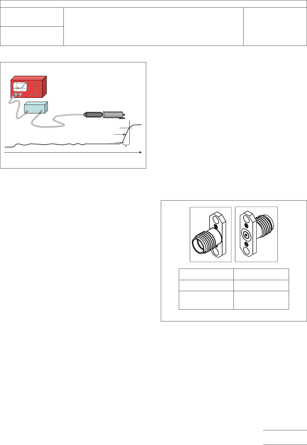
4.4.5 TDR Risetime Requirement The procedure
depicted in Figure 4-5 can be used to determine the rise time
or maximum slope of the TDR measurement system through
the probe tip. This is done to ensure that there is sufficient
high frequency content within the step pulse that is to be
injected into the device under test (DUT) for the respective test
method.
Note: The SIU is a static isolation unit designed to eliminate
static damage to the TDR sampling head. It may be included
within the TDR instrumentation.
4.4.5.1 EBW Risetime The rise time (10%-90%) for EBW
shall contain sufficient spectral content as agreed upon
between vendor and customer base on the printed board
application with the open tip of the probe. For EBW, hold the
probe in air see Figure 4-5 and measure the maximum slope
of the rise time of the step response (in Megavolts/second)
and/or the risetime. This value should be compared to the
IPC-TM-650
Number
2.5.5.12
Subject
Test Methods to Determine the Amount of Signal Loss on
Printed Boards
Date
07/12
Revision
A
Page 10 of 24
EBW requirements agreed upon between customer and ven-
dor.
4.4.5.2 RIE Risetime The rise time (10%-90%) for RIE
shall be 250 ps or as agreed upon between vendor and cus-
tomer with an open tip of the probe as illustrated in Figure 4-5.
4.4.5.3 SPP Risetime The rise time (10%-90%) for SPP
shall be 11 to 35 ps or less at the open tip of the probe or
cable connector as illustrated in Figure 4-5. SPP has an addi-
tional requirement of an impulse forming network to be
located between the TDR head and the test probe.
4.4.5.4 SET2DIL Risetime The rise time (10-90%) for
SET2DIL shall be <35 ps at the open tip of the probe or cable
connector as illustrated in Figure 4-5.
4.4.6 TDR Impedance The impedance of the TDR unit
should be 50 Ω with an impedance uncertainty less than or
equal to ± 0.5 Ω.
4.4.7 TDR System Calibration Follow the TDR instrument
manufacturer’s recommendation for the frequency of factory
calibration. Since RIE is related to the ratio of loss, field cali-
bration reverts to insuring proper results from calibration stan-
dards.
4.4.8 SPP Impulse Forming Network Requirement The
pulse width at the output of the IFN observed at the probe tip
shall be a minimum of 20 ps. The recommendation is to have
a 20 ps to 60 ps pulse width detected in TDT through the
measurement set-up on typical line lengths used in the test
coupon.
4.4.9 Printed Board Connectors The TDR cable connec-
tion shall utilize a ‘‘SMA,’’ 3.50 mm, or 2.92 mm connectors
at their measurement ports. It is recommended that cable
connections be tightened with a torque wrench to follow
specifications, unless otherwise specified by the manufacturer
of the connector or cable.
Three general probing solutions may be utilized to perform the
SPP extraction: microprobe pads, SMA connectors, and
handheld probes. Surface-mounted SMAs, as shown in Fig-
ure 4-6, are recommended for SPP. They may be either
bolted or slip-fitted into the alignment holes as explained ear-
lier. The bolt-down specification for a Molex SMA style con-
nector, part number 73251-1850, is shown in Figure 4-6.
4.4.10 TDR Cabling All test cables shall meet the follow-
ing minimum specifications:
a) Coaxial with a 50 ±1 Ω characteristic impedance
b) 2.92 mm, 3.50 mm, or SMA connectors
c) Max cable insertion loss ≤2.50 dB at 65 GHz, 50 GHz,
40 GHz, or 26.5 GHz, respectively
d) Probing insertion loss ≤0.33 dB at 65 GHz, 50 GHz,
40 GHz, or 26.5 GHz, respectively
IPC-25512-4-5
Figure 4-5 Measurement of Maximum Slope of Step
Risetime at Open End of Probe
TDR Instrument
probe
SIU
Maximum
risetime
Rise time
Time
IPC-25512-4-6
Figure 4-6 Bolt Down Torque Requirement for 2
Connector Styles
Connecter Type Required Torque
SMA 5 in-lb (0.56 N-m)
3.50 mm
2.92 mm
8 in-lb (0.90 N-m)
IPC-TM-650
Number
2.5.5.12
Subject
Test Methods to Determine the Amount of Signal Loss on
Printed Boards
Date
07/12
Revision
A
Page 11 of 24
4.4.11 TDR ESD Protection TDR equipment shall pro-
vide ESD protection commensurate with the test environment.
It is recommended that samples be grounded to remove any
residual static to protect against static discharge with in the
test environments.
Static can be built up on samples prior to test and can dam-
age the sampling heads in the TDR/TDT equipment. There-
fore, it is recommended that ESD protection be used. Such
protection must be supplied internally to the TDR system.
Samples should be grounded to remove any residual static
and/or passed through some type of deionization device prior
to testing. This can be done by shorting each line to ground
with a simple connection between one end of the lines and
the instrument ground. Keeping the relative humidity in the
test area between 45% and 55% may minimize the buildup of
static. Operators are always required to have a grounding
strap around one wrist havinga1MΩ resistor in series with it.
Special waxing can be used on the lab floor to prevent body
charge build-up. Always use a grounded, conductive table
mat. Always wear a heel strap. Always ground the center con-
ductor of a test cable before making a connection to static-
sensitive equipment.
4.5 SPP Test Apparatus
4.5.1 Other SPP Equipment Requirements
An LCR
meter is required that can measure capacitance at 1 MHz.
4.5.2 SPP Software The following software is required for
implementation of the SPP technique:
a) Gamma-Z software for signal processing or equivalent
b) 2D field solver such as CZ2D, which can be downloaded
from: www.alphaworks.ibm.com/tech/gammazandcz2d,
or equivalent
4.6 FD Test Apparatus The measurement equipment
needed includes a VNA, cabling, a probing solution, and a
calibration structure and calibration coefficients that are
acquired from the probe or connector manufacturer. The
probing solution should match the test sample chosen from
the above described samples. High performance connectors
and cables are recommended in performing VNA measure-
ments. Optionally, a TDT system may be used in place of a
VNA to acquire frequency domain attenuation and loss data.
5 Procedures
5.1 EBW Measurements Procedure
5.1.1 Measurement Process
This procedure will measure
the maximum slope of the rise time of the combined measure-
ment system and DUT and determine a loss factor. Recom-
mended resolution is 4000 points with a horizontal scale of
200 ps/div.
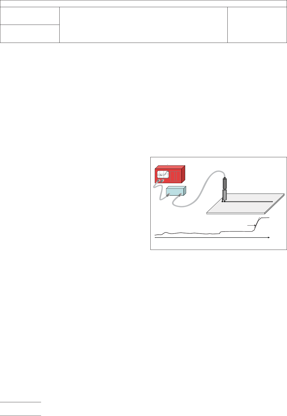
Step 1 – Probe the interconnect (see Figure 5-1) and measure
the maximum slope of the step response in Megavolts/second
(e.g., 430 Megavolts/second). The maximum slope may be
directly acquired from TDR equipment with that capability.
Step 2 – Report the Loss Factor at the test system bandwidth
(as measured within 4.4.5.1) (e.g., 430 Megavolts/second @
14.5 GHz).
5.2 RIE Measurement Procedures Figure 5-2 summa-
rizes the RIE measurement procedure.
The RIE method utilizes a comparison between a reference
loss (line) measurement and a test conductor (line) measure-
ment. The reference measurement may be a calibration stan-
dard or short length of conductor in the neighborhood and on
the same layer as the conductor to be measured.
5.2.1 TDR – Open or Unterminated Line Requirement
The RIE method requires a measurement of lines where one
end is a probe launch and the other end is left unterminated
or open. The probe injects a fast step at the launch point in
much the same manner specified in IPC-TM-650, Method
2.5.5.7. The injected step causes a wave to propagate down
the line; most of the wave is reflected by the open end of the
line and travels back to the source where it is measured as the
superposition of the incident wave and all the reflections.
IPC-25512-5-1
Figure 5-1 Measurement of Maximum Slope of Step Rise
Time at Open end of DUT
TDR Instrument
probe
SIU
Maximum
risetime
DUT
(interconnect)
Time
IPC-TM-650
Number
2.5.5.12
Subject
Test Methods to Determine the Amount of Signal Loss on
Printed Boards
Date
07/12
Revision
A
Page 12 of 24