IPC-TM-650 EN 2022 试验方法.pdf - 第718页
1 Scope This test method is used to determine the ability of a polymer solder mask protective coating to withstand an environment conducive to electrochemical migration. 2 Applicable Documents IPC-A-25A-G-KIT 1 Multipurp…

separate
measurements are needed to obtain a statistically
meaningful result.
6.0
PWB Process Test/Sampling
For testing of lot con-
formity at least ten different PWBs with parallel conductors as
per Section 3 shall be tested.
7.0
Test Interpretation
Test
for susceptibility to metallic
dendritic growth is a relative measure of localized ionic residue
levels. As such, it does not have direct relationship with abso-
lute PWB reliability measure. The results of this test are found
useful in the PWB process control by testing board-to-board
and lot-to-lot variations.
IPC-TM-650
Number
2.6.13
Subject
Assessment
of Susceptibility to Metallic Dendritic Growth:
Uncoated Printed Wiring
Date
10/85
Revision
P
age2of2
电子技术应用 www.ChinaAET.com
1 Scope This test method is used to determine the ability of
a polymer solder mask protective coating to withstand an
environment conducive to electrochemical migration.
2 Applicable Documents
IPC-A-25A-G-KIT
1
Multipurpose One-Sided Test Pattern -
Gerber Format
IPC-SM-840 Qualification and Performance of Permanent
Solder Mask
IPC-TR-476 Electrochemical Migration: Electrically Induced
Failures in Printed Wiring Assemblies
J-STD-004 Requirements for Soldering Fluxes
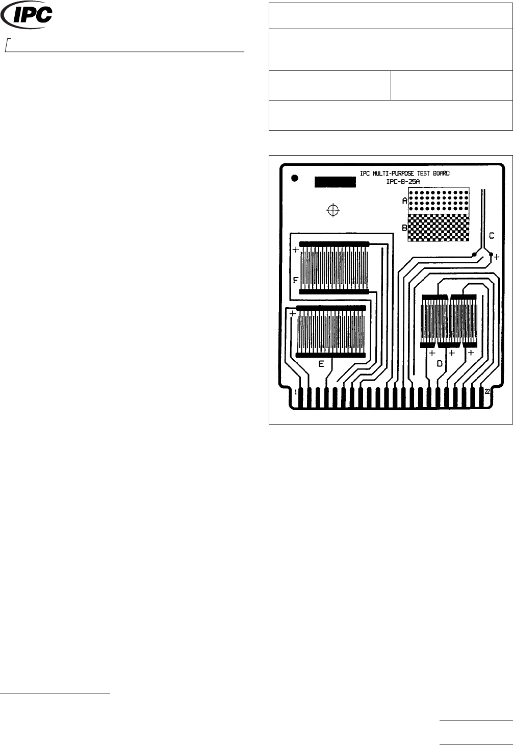
3 Test Specimens The IPC-A-25A-G-KIT artwork package
provides the Gerber files necessary for the fabrication of the
standard IPC-B-25A test board used with this test method.
3.1 Qualification Testing Three IPC-B-25A boards (see
Figure 1) using the D comb patterns with 0.32 mm [0.0126 in]
lines and spaces for both Classes T and H, coated with sol-
der mask according to the solder mask supplier’s recommen-
dations.
3.2 Conformance Testing Three IPC-B-25A boards (see
Figure 1) using the C comb pattern (‘‘Y’’ shape pattern) which
should be 0.64 mm lines/0.64 mm spacing [0.025 in lines/
0.025 in spacing] or the pattern with the minimum spacing on
the production board, whichever has the smallest line spac-
ing, coated with solder mask according to the solder mask
supplier’s recommendations.
4 Equipment/Apparatus
4.1 Power Supply
Capable of supplying 10 ± 0.5 VDC at
1 A, maximum.
4.2 Oven Capable of maintaining up to 90±1°C[194 ±
1.8 °F].
4.3 Chamber Capable of maintaining 85±2°C[185 ± 3.6
°F] with 85%, minimum, relative humidity.
4.4 Desiccator 25 cm [9.84 in] diameter minimum, with
openings for the connecting wires to pass through while main-
taining a hermetic seal.
4.5 Potassium Sulfate Reagent Grade potassium sulfate.
4.6 RTV Dow Corning 732 RTV potting compound or
equivalent.
4.7 Resistors 10 megohm resistor for Class H testing and
1 megohm resistors for Class T testing
4.8 Magnifier Capable of supplying 10X magnification
4.9 Soldering Iron
1. www.ipc.org/onlinestore
IPC-2614-1
Figure 1 IPC-B-25A Test Board
3000 Lakeside Drive, Suite 309S
Bannockburn, IL 60015-1249
IPC-TM-650
TEST METHODS MANUAL
Number
2.6.14
Subject
Solder Mask - Resistance to Electrochemical
Migration
Date
03/07
Revision
D
Originating Task Group
Solder Mask Performance Task Group (5-33b)
Material in this Test Methods Manual was voluntarily established by Technical Committees of IPC. This material is advisory only
and its use or adaptation is entirely voluntary. IPC disclaims all liability of any kind as to the use, application, or adaptation of this
material. Users are also wholly responsible for protecting themselves against all claims or liabilities for patent infringement.
Equipment referenced is for the convenience of the user and does not imply endorsement by IPC.
Page1of4
ASSOCIATION CONNECTING
ELECTRONICS INDUSTRIES
®

4.10 Flux Water white rosin (R or RMA) with halide content
less than 0.5%, i.e., type Symbol A and B or ROL0 and ROL1
according to J-STD-004.
5 Test Conditions
5.1.1 Class T
85±2°C[185 ± 3.6 °F] with 85% relative
humidity minimum, 10 VDC bias, for 500 hours.
5.1.2 Class H 85±2°C[185 ± 3.6 °F] with 90, +5/-0%
relative humidity, 10 VDC bias for 168 hours.
5.2 Specimen Preparation
5.2.1
Positive, permanent and noncontaminating identifica-
tion of the test specimens is of paramount importance.
5.2.2 Visually inspect the test specimens for any obvious
defects, as described in IPC-A-600. If there is any doubt
about the overall quality of any test specimen, the test speci-
men should be discarded.
5.3 Electrical Connections (Both Classes)
5.3.1
For qualification testing, solder single strand PTFE
insulated wires or equivalent to the lands of each of the D test
patterns using a noncontact shield to protect the patterns
from flux splattering. These wires will be used to connect the
test specimen to the bias voltage or resistance meter. Test
points 1, 3 and 5 are to be connected to the positive terminal
and test points 2 and 4 are to the negative terminal of resis-
tance meter or power supply. When resistors are used, they
are to be connected between test points 1, 3 and 5 and the
positive terminal of power supply.
5.3.2 For conformance testing, solder single strand PTFE
insulated wires or equivalent in each of the connecting points
of the pattern described in 3.2 using a noncontact shield to
protect the patterns from flux splattering. These wires will be
used to connect the test specimen to the bias voltage or
resistance meter. One side of the pattern should be con-
nected to the positive terminal and the other side to the nega-
tive terminal of resistance meter or power supply. When resis-
tors are used, they are to be connected between the pattern
and the positive terminal of power supply.
5.3.3 The flux shall not be removed from the test speci-
mens.
5.4 Procedures
5.4.1 Desiccator Test Method
5.4.2
Take insulation resistance measurements of the test
specimens using 10 VDC, prior to testing. This step will
ensure that the resistance measurements are sufficient to pro-
ceed with testing.
5.4.3 Prepare a saturated solution of distilled water and
potassium sulfate (approximately 35g per 100 mL) at a tem-
perature of 85 °C [185 °F]. Pour the solution into the desicca-
tor just below the ceramic plate. Crystals of potassium sulfate
should remain visible in the saturated solution in the oven at
operating temperature.
5.4.4 Place the test specimens into the desiccator, such
that they do not touch one another. Route the connecting
wires to the outside of the desiccator and seal with a silicone
potting compound such as Dow Corning 732 RTV or a heat
resistant vacuum grease.
5.4.5 Place the desiccator into an oven maintained at 85 °C
[185 °F]. For the remaining test procedures, see 5.5.4 to 5.6.2
for Class H and 5.7.4 to 5.8.4 for Class T.
5.5 Class H – Test Chamber Method
5.5.1
Prior to testing, take insulation resistance measure-
ments of the test specimens using 10 VDC. This step will
ensure that the resistance measurements are sufficient to pro-
ceed with testing.
5.5.2 Place the specimens into the test chamber and route
the wires through the porthole of the test chamber and seal, if
necessary.
5.5.3 Set the chamber’s parameters, which is a noncon-
densing ramp, for 85 °C [185 °F] with 90% relative humidity.
Close the chamber doors and activate the test chamber.
5.5.4 Connect the correct test points as specified in 5.3.1
and 5.3.2 to a 10-megohm resistor before the positive termi-
nal of power supply. (See Figure 2 for configuration for quali-
fication testing.) Apply the bias voltage of 10 VDC.
5.5.5 Allow the test specimens to remain in the test cham-
ber for the duration of 168 hours (seven days).
IPC-TM-650
Number
2.6.14
Subject
Solder Mask - Resistance to Electrochemical Migration
Date
03/07
Revision
D
Page2of4