IPC-TM-650 EN 2022 试验方法.pdf - 第562页
IPC-TM-650 Number Subject Date Revision Page 3 of 7 2.5.5.15 Relative Permittivity and Loss Tangent Using a 06/22 Split- Post Dielectric Resonator N/A 4 Apparatus or Material 4.1 Test System The schematic diagram of the …
IPC-TM-650
Number Subject Date
Revision
where
h
g
is the distance between the metal enclosures of the fixture;
D is internal diameter of the metal enclosures;
L is internal height of the metal enclosures;
d
r
is the diameter of the dielectric resonator;
h
r
is the thickness of the dielectric resonator.
3.3 Specimen Thickness The thicker the specimen the less error occurs in the measurements. A thin specimen may be stacked
up to a minimum of 0.4 mm [0.016 in] to improve measurement accuracy. The air gaps between the sample and the fixture do
not affect the measurement.
3.4 Number of Specimens Three specimens for the test at room temperature and one specimen for the test at variable temperatures
are required for each SPDR test fixture for this test. Table 1 shows the supported specimen dimensions
Table 1 – Specimen Dimensions
Nominal Frequency [GHz]
Specimen Sizes
mm [inch]
Maximum Thickness
mm [inch]
1 150 X 150 [5.9 X 5.9] 6.0 [0.24]
3 80 X 80 [3.2 X 3.2] 3.0 [0.12]
5 to 6 80 X 80 [3.2 X 3.2] 2.0 [0.08]
9 to 10 80 X 80 [3.2 X 3.2]
0.9 [0.035]
13 to 16 50 X 35 [2.0 X 1.4] 0.6 [0.024]
18 to 20 15 X 15 [0.6 X 0.6] 0.5 [0.020]
2.5.5.15 Relative Permittivity and Loss Tangent Using a 06/22
Split-Post Dielectric Resonator
N/A
Page 2 of 7
IPC-TM-650
Number Subject Date
Revision
Page 3 of 7
2.5.5.15 Relative Permittivity and Loss Tangent Using a 06/22
Split-Post Dielectric Resonator
N/A
4 Apparatus or Material
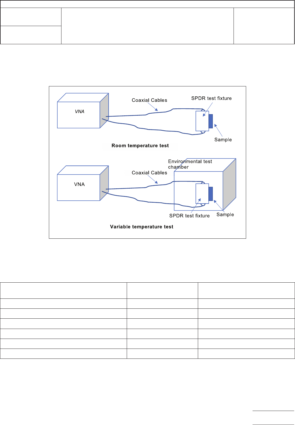
4.1 Test System The schematic diagram of the test system is shown in Figure 2. The test can be conducted at room temperature
or an elevated temperature as indicated.
Figure 2 – Schematic Diagram of Test System
4.2 Test Fixture Parameters Table 2 shows the typical relationship between the SPDR test fixture’s nominal frequency and
h
g
and D. For different test frequencies, the corresponding SPDR test fixture of nominal frequency shall be used.
Table 2 – Test Fixture Configurations
SPDR Test Frequency
[GHz]
D
mm [inch]
hg
mm [inch]
1 120 [4.7] 6.0 [0.24]
3 50 [2.0] 3.0 [0.12]
5 to 6 30 [1.2] 2.0 [0.08]
9 to 10 22 [0.9] 0.9 [0.035]
13 to 16 15 [0.6] 0.6 [0.024]
18 to 20 10 [0.4] 0.5 [0.020]
4.3 Vector Network Analyzer (VNA) The frequency range of the VNA shall be 500 MHz to 20 GHz, The dynamic range of the
VNA shall be more than 60 dB.
4.4 Calibration Reference The calibration equipment shall include a standard reference sample. For example, a single-crystal
quartz or equivalent reference, and a calibration assembly for the VNA.
IPC-TM-650
Number Subject Date
Revision
4.5 Micrometer A micrometer with a minimal resolution of 0.001mm [0.00004 inch] or better.
4.6 Circulating Oven An air circulating oven with capable of a temperature of 105 ± 1 °C [221 ± 1.8 °F].
4.7 Test Chamber A test chamber for variable temperature testing capable of a range of -125 °C to +110 °C [-193 to +230 °F]. Other
temperature ranges may be used as agreed between user and supplier. Temperature accuracy must be ± 1 °C ( ± 1.8 °F) of actual set
point.
5 Procedure
5.1 Preconditioning All specimens shall be conditioned at 23 ± 2 °C [73.4 ± 3.6 °C] and 50 ± 5 % RH for a minimum of 24 hour after
etching and prior to testing.
5.2 Testing of relative permittivity and loss tangent at room temperature
5.2.1 The ambient test temperature should be 23 °C ± 2 °C [73.4 ± 3.6 °F]. The variation should not exceed ± 1 °C [± 1.8 °F] during
the test. Allow a minimum of 30 minutes for the VNA to warm up and stabilize.
5.2.2 Select a SPDR test fixture in accordance with the test frequency. The specimen size and thickness shall comply with the
requirements specified in Table 1. For example, if the test frequency is 10 GHz, a SPDR test fixture with 10 GHz nominal frequency
should be selected. The supported specimen size is 80 mm × 80 mm [3.2 X 3.2 inch] and the maximum thickness of specimens is no
more than 0.9 mm [0.035 inch].
5.2.3 Connect the SPDR test fixture to VNA. The test fixture shall be kept horizontal. Set the VNA parameters according to the
manufacturer’s instructions and the nominal frequency of the SPDR fixture.
5.2.4 Measure resonance frequency (f
0
) and Q-factor (Q
0
) values of the empty resonator.
5.2.5 Utilize a micrometer to measure the thickness of the specimen and record as h. Insert the specimen into the test fixture. The side
with marking is face up and the edge of this side has to be aligned with the fixture edge.
5.2.6 Measure the resonance frequency (f
s
) and Q-factor (Q
s
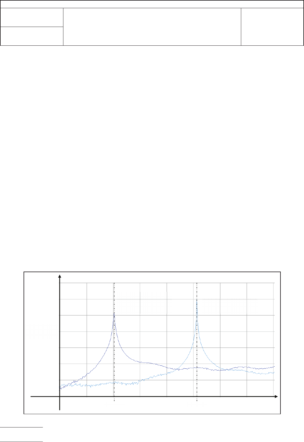
) of the resonator containing the specimen. A plot of the change of
resonance frequency with or without the specimen is shown in Figure 3.
Resonance
amplitude
f
r
f
Resonance
frequency
0
Empty resonator
Resonator
containing the
specimen
Figure 3 – Plot Showing Change of Resonance Frequency
2.5.5.15 Relative Permittivity and Loss Tangent Using a 06/22
Split-Post Dielectric Resonator
N/A
Page 4 of 7