IPC-TM-650 EN 2022 试验方法.pdf - 第436页
The test pattern card shall have a permittivity equal to the nominal value of the type being tested with a tolerance of ± 2.5% of the nominal value (measured by stacking sufficient plies to the total thickness requiremen…

•
Sweep Frequency Generator Mainframe H.P. 8350B
• RF Plug-In, 0.01 to 20 GHz H.P. 83592A. A plug-in of nar-
rower frequency range (X-band) may be selected at consid-
erable cost savings. 83545A 5.9 12.4 GHz.
• Power Splitter H.P. 11667A
• Automatic Frequency Counter H.P. 5343A
• Source Synchronizer H.P. 5344A. Obtained as an intercon-
nected assembly with the counter.
• Coaxial cables and adapters.
• 10 dB Attenuator H.P. 8491B
• 8.9 kN Dillon Force Gauge, Compression Model X, Part
Number 381612301, with ±1% full scale accuracy.
• Vise or press that is able to exert controlled 4.45 kN force
on the test fixture and that opens at least 127 mm to accept
the force gauge and test fixture.
• Programmable Power Meter H.P. 436A
• Power Sensor H.P. 8484A with 70 to 10 dBm range.
• IEEE 488 (GPIB) cables
• Controlling computer with GPIB interface.
The above equipment is connected as follows as illustrated in
Figure 2:
• RF connections. The power splitter connects directly to the
RF plug-in output. One output of the splitter connects by RF
cable to the counter input. The other output is connected by
RF cable to the attenuator which connects to one of the test
fixture probe lines.
• Control connections. Connections between counter and
synchronizer are provided as specified by the manufacturer.
The FM output from the synchronizer connects by BNC to
the FM input on the sweeper. GPIB cables connect in par-
allel to sweeper, synchronizer, power meter, and computer
interface.
• Other connections. The power sensor is connected to the
other probe of the fixture and its special cable connects into
the power meter.
• A synthesized CW generator can be used to replace the
sweeper, plug-in, power splitter, connector, and source syn-
chronizer for the simpler set-up shown in Figure 3.
4.3
Automated Network Analyzer for the Test Setup
The
instrumentation described in 4.1 or 4.2 may be replaced
with either a scalar or vector network analyzer with test cables
connected to the test fixture of 5.0 as the device under test
(DUT). Examples of automated network analyzers known to
be suitable include the Hewlett-Packard 8510 vector network
analyzer or the Wiltron Model 561 scalar network analyzer.
These or equivalent may be used.
Such instruments may be operated either manually or under
computer control with suitable programming to locate the
resonant frequency and the frequencies above and below
resonance where transmitted power is 3 dB below that at
resonance. Network analyzers have several advantages over
the instrumentation described in 4.1 and 4.2. Data collection
is rapid and may be continuously refreshed with averaging.
The log magnitude response curve for ratio of transmitted to
incident power (the S21 parameter) as dB versus frequency is
visible on a screen for easy verification of a valid resonance. A
large number of dB frequency data points near the resonance
are readily available for optional use of non-linear regression
analysis techniques to determine the frequency and Q values
with statistically better degrees of uncertainty than those
attainable by the three point (f
r
,f
1
and
f
2
)
method in either
section 6.2 or 6.3.
5.0
Test Fixture
5.1 Recommended Fixture Design
An
improved test fix-
ture design is shown that facilitates changing test pattern
cards and lends itself to control of temperature. The test fix-
ture shall be constructed as shown in Figure 4 through Figure
14.
The resonator circuit shown in Figure 4 is an example of a test
pattern designed for a material with a permittivity of 2.20. For
other permittivity values, different pattern dimensions will be
required as outlined in Table 1. It shall be defined on one side
of a material of similar type to that being tested, a laminate
with dielectric thickness of 0.216 mm ± .018 mm. The clad-
ding thickness is normally specified as MF-150F designation 1
copper (nominal thickness of 0.036 mm but designation down
to Q (0.010 mm) may also be used. Designation Q is preferred
for high permittivity materials as covered in 4.2 and 9.7, Note.
The reverse side of the circuit board has all copper removed.
The copper foil shall be of IPC-MF-150, type 1, electro-
deposited, type 5, wrought, or type 7, wrought-annealed. The
type of copper foil and the treatment for adhesion will affect
the Q measurement. The 1/Qc values in Table 1 do not take
into account surface treatments or higher resistivity values for
the conductor that are encountered with the specified foil
types.
IPC-TM-650
Number
2.5.5.5
Subject
Stripline
Test for Permittivity and Loss Tangent (Dielectric Constant
and Dissipation Factor) at X-Band
Date
3/98
Revision
C
P
age3of25
电子技术应用 www.ChinaAET.com

The
test pattern card shall have a permittivity equal to the
nominal value of the type being tested with a tolerance of ±
2.5% of the nominal value (measured by stacking sufficient
plies to the total thickness requirement of a specimen as
above. Use a photo resist and etching method capable of
reproducing circuit dimensions with ± 0.025 mm tolerance. All
copper shall be removed from the other side of the test pat-
tern card. See 9.7, Note, for special treatment of ceramic-
PTFE substrate types.
The pattern card of Figure 4 is 68.6 mm wide by 55.4 mm
high and is designed for the fixture hardware in Figure 5
through Figure 14. The length is cut so that when the pattern
card is clamped for the lap joint with the striplines on the base
card, the resonator is centered in the 51 mm high area above
the base plates of the fixture. For materials with permittivity
values higher than the nominal 2.50 shown in Table 1, please
see 5.2 for a discussion of recommended fixture modifica-
tions.
Probe line widths are based on ground plane spacing taken
as twice the nominal thickness of the two specimens plus
thickness of the pattern card and its 0.034 mm copper foil
pattern and computed as if the stripline were centered
between ground planes
(1,3)
.
Chamfer
values are based on published design curves
(2)
.
The
length of the four node resonator is given in Table 1.
Resonators of lower node values for the purpose of measur-
ing ∆L according to 6.1, will be proportionately shorter with
the probe lengths modified so that the gap is the same.
The values for conductor loss, 1/Q
c
,
in Table 1 are calculated
from known properties of copper, the test frequency, the cal-
culated characteristic impedance of the section of stripline
comprising the resonator, and its cross-sectional geometry
using published formulas
(1)
.
The values shown are usually
biased low giving a high bias to loss tangent results, because
conductor actually used may not have a smooth surface and
may include oxides, microvoids, or other sources of higher
resistivity.
5.2
Fixture Modifications for High Permittivity Materi-
als
Modification
of the fixture design of Figure 5 through Fig-
ure 14 and pattern card dimensions in Figure 4 are recom-
mended to overcome problems experienced with extraneous
transmissions and resonances at frequencies near the desired
resonant peak.
5.2.1 Replace
the coax-stripline launcher shown in Figure 7.
The part suggested has a tab width of 1.27 mm and may be
replaced with Omni-Spectra Part No. 2070-5029-02, or
equivalent, intended for 1.57 mm ground plane spacing and
with a tab width of 0.635 mm. A further acceptable alternative
is to redesign the base plates to accept another type of
coaxial fitting such as a flange mount jack, which can be
modified to provide a smooth, low-reflection transition from
3.0 mm semirigid cable with Z
0
=
50 Ohm, low permittivity
insulation into stripline with Z
0
=
50 Ohm, and high permittiv-
ity insulation in the fixture.
5.2.2
If
the stripline launcher in 5.2.1 is used, the edge at
the step to accommodate the launcher body on the base
plate should be machined with a slight undercut for an acute
included angle of about 80°. This, combined with a means to
press the launcher body axially against the edge, will assure a
well-defined ground connection from coax to stripline. A
poorly defined ground connection with ground current path
length varying or longer than that of the signal conductor has
been found to give rise to scattering, reflections, and reso-
nances in the open ended probe line that are evident as extra-
neous fixture transmissions that may distort the resonant peak
to be measured.
5.2.3
Omit
the conductor lap joints but keep the extended
base cards in the fixture assembly. See figures 13 and 14.
With high permittivity materials, the lap joint also gives rise to
unwanted scattering, reflections, and resonances in the open-
ended probe line, as discussed in 5.2.2. For this purpose the
resonator pattern card will have a longer vertical dimension to
extend down to the launcher pin replacing the spacer board
in Figure 13. It should still center the resonator in the clamp-
ing block area. The base dielectric boards will be etched free
of metal. The ground plane foils will also extend down to the
launcher.
The feature of extending the base dielectric boards upward
above the base plates is to be retained as a means to prevent
premature damage to the resonator pattern card with
repeated loading and unloading of the fixture. The base plate
with the deeper step will be on the side toward which the
resonator pattern faces to avoid straining the offset launcher
tab during assembly.
5.2.4
Scale
down the fixture dimensions to move remaining
probe line resonances away from the resonant frequency of
interest. For ε
r
=
10.5 material, the following dimensions were
found effective.
IPC-TM-650
Number
2.5.5.5
Subject
Stripline
Test for Permittivity and Loss Tangent (Dielectric Constant
and Dissipation Factor) at X-Band
Date
3/98
Revision
C
P
age4of25
电子技术应用 www.ChinaAET.com
Height
of base plate from step to top edge
Height of clamp block and specimen
Height from launcher body to resonator
center line
Width of clamp block and specimen
Horizontal center line distance between
probe lines
Probe length from launch to gap
mm
8.53
25.4
21.23
55.9
30.5
25.81
5.2.5 Thinner
copper cladding (weight Q) for the resonator
pattern card is recommended as mentioned in 5.1. If weight
Q is used, the embedding process discussed in note 9.7 can
be avoided. Experience has indicated that this reduction in
thickness has not impaired the loss tangent values obtained
by the method.
5.3
Older Fixture Design
An
older acceptable alternate
test fixture design is shown in Figure 15. This is included since
fixtures of this type are in service at various laboratories. Com-
pared to 5.1, fixtures of this design depend on ambient con-
ditions for temperature control. Changing resonator test pat-
tern cards is less convenient.
5.4
Temperature Control
It
is a well-known fact that PTFE
and composites containing it show a room temperature tran-
sition in the crystalline structure that produces a step-like
change in the permittivity. This temperature region should be
avoided.
Normally, control of ambient temperature is adequate for rou-
tine measurements. A means other than ambient temperature
to control fixture temperature facilitates collecting data on the
variation of permittivity with temperature. With the test fixture
of 5.1., use 6 mm inside diameter tubing for circulating fluid to
control temperature. The following items are needed to com-
plete the temperature control system.
5.4.1
Laboratory
Immersion Heating Bath/Circulator, such
as Haake Model D1, Lauda Model MT, or equivalent and a
small capacity bath. The Immersion Heating Bath/Circulator
shall be connected to the clamping blocks in series with a
return line to the bath.
5.4.2
Two
fine diameter thermocouple probes with leads
and suitable instrumentation for readout or recording of tem-
perature. A digital thermometer, such as Ohmega Model DSS
115 or equivalent, is used for monitoring temperature.
6.0
Measuring Procedure
6.1 Preparation for Testing
The
actual length of the reso-
nator element shall be determined by an optical comparator or
other means capable of accuracy to 0.005 mm or smaller.
Unless otherwise specified, specimens shall be stored before
testing at 23°C + 1-5°C/50% ± 5% relative humidity (RH). The
referee minimum storage time is 16 hours. Shorter times may
be used if they can be shown to yield equivalent test results.
If electronic equipment, as listed in 4.2, is used, it shall be
turned on at least one half hour before use to allow warm-up
and stabilization. The automatic frequency counter listed in
4.2 is provided with temperature control of the clock crystal
that operates even when the power switch is off. Care should
T
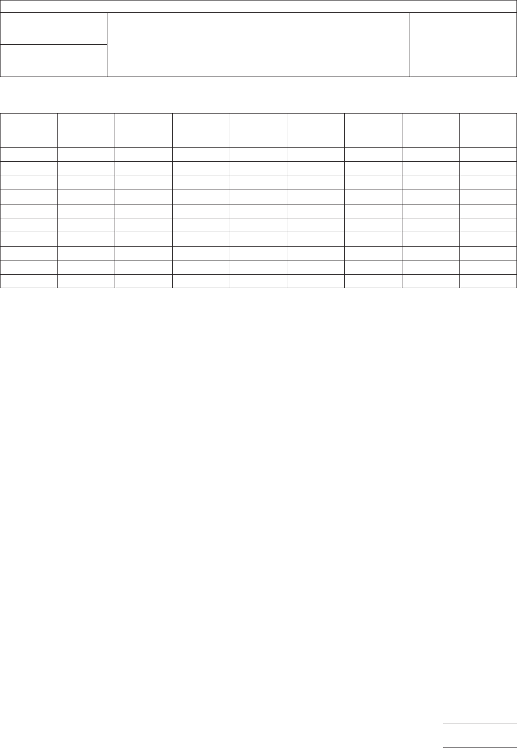
able 1 Dimensions for Stripline Test Pattern Cards in Millimeters
Nom. ε
r
Nom.
Thk.
Pattern
Card
Thk.
Probe
Width
Chamfer
X, Y
Probe
Gap
Resonator
Width
Resonator
Length 4
Node
1/Q
C
Conductor
Loss
2.20
1.59 0.22 2.74 3.05 2.54 6.35 38.1 0.00055
2.33 1.59 0.22 2.67 2.92 2.54 6.35 38.1 0.00055
2.50 1.59 0.22 2.49 2.79 2.54 6.35 38.1 0.00055
3.0 1.59 0.22 2.13 2.41 2.54 5.08 31.8 0.00058
3.5 1.59 0.22 1.85 2.16 2.54 5.08 31.8 0.00058
4.0 1.59 0.22 1.62 1.93 2.54 5.08 31.8 0.00058
4.5 1.59 0.22 1.45 1.73 2.54 5.08 31.8 0.00058
6.0 1.59 0.22 1.07 1.30 2.29 3.81 25.4 0.00062
6.0 1.27 0.22 0.86 1.07 2.29 3.81 25.4 0.00072
10.5 1.27 0.22 0.41 0.54 2.03 2.54 17.3 0.00079
Standard
clamp force for all the above is 4.45 ± 0.22 kN
IPC-TM-650
Number
2.5.5.5
Subject
Stripline
Test for Permittivity and Loss Tangent (Dielectric Constant
and Dissipation Factor) at X-Band
Date
3/98
Revision
C
P
age5of25
电子技术应用 www.ChinaAET.com