IPC-TM-650 EN 2022 试验方法.pdf - 第674页
4.2 A resistance meter capable of reading high resistance (10 12 ohms) with a test voltage of 100 ± 2 volts DC or an ammeter capable of reading 10 -10 amperes in combination with 100 volts DC power supply. Standard resis…
1
Scope
This
test method is used to characterize the
cleanliness of printed wiring board fabrication processes by
determining the degradation of electrical insulation resistance
under conditions of high temperature and humidity.
This test method examines the cleanliness of a test substrate
prior to solder mask application, after solder mask application,
and after any final metalization and/or surface finish operation
(e.g., HASL or OSP), and may be used to demonstrate the
cleanliness of internal layers of a mulitilayer board prior to
lamination.
2
Applicable Documents
GR-78-CORE
Telcordia
Technologies (Formerly Bellcore)
2.1
Master Drawings
Telcordia
Technologies Test Pattern (GR-78-CORE, Figures
14.1 and 14.2)
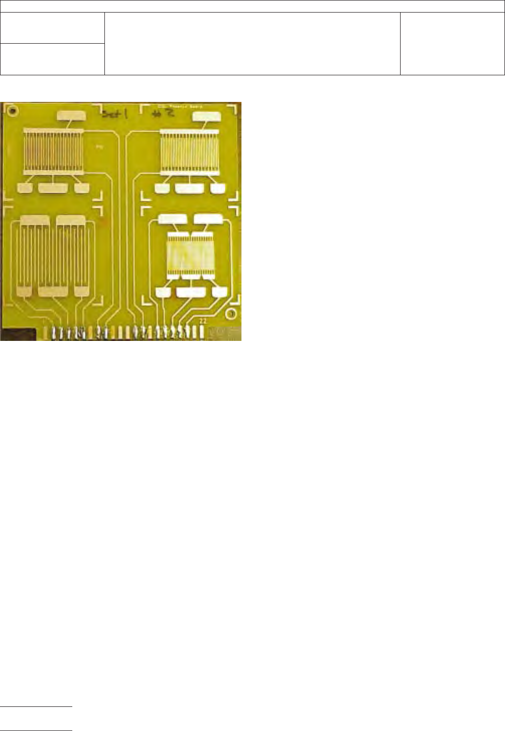
IPC-B-50 Standard Test Board (Figure 3)
3
Test Specimens
The
test specimen for this test method
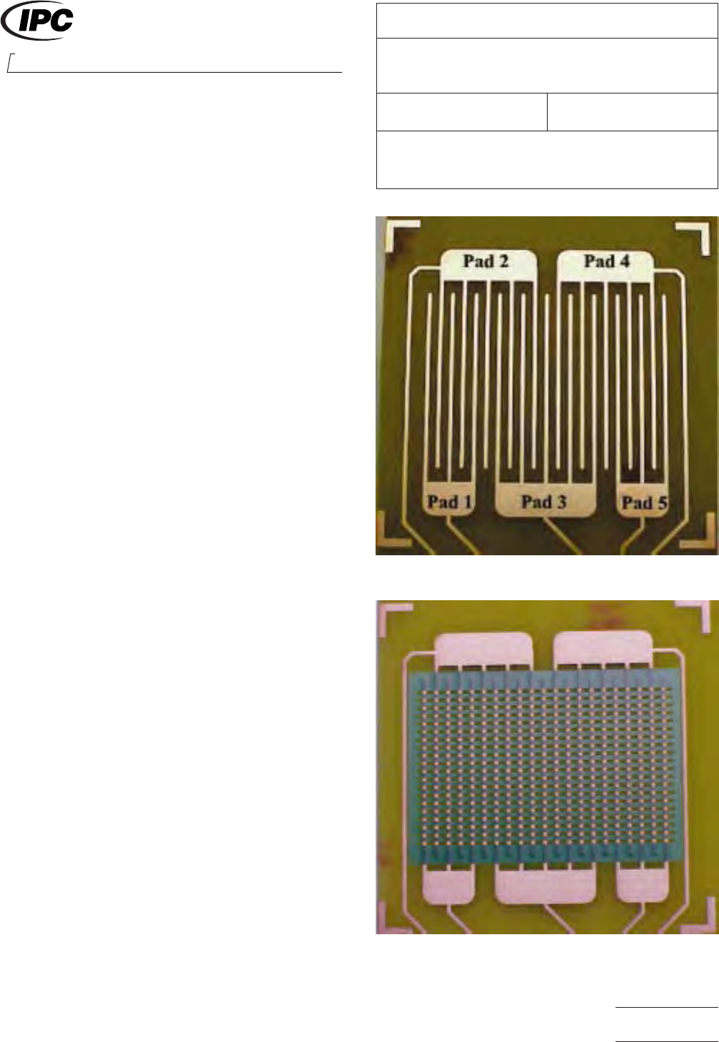
is the interdigitated comb pattern shown in Figures 1 and 2.
This test pattern can be produced in a number of formats, but
exists as one of the stock patterns of the IPC-B-50 standard
test board (see Figure 3).
This comb pattern has 0.65 mm [0.025 in] lines and 1.27 mm
[0.050 in] spacings. This test pattern is also commonly
referred to as the Bellcore pattern. When used for qualification
purposes, the base laminate will be FR-4 epoxy-glass with
17 µm [0.5 oz equivalent] unprotected copper metalization.
4
Apparatus
4.1
Clean
test chamber capable of producing and recording
an environment of 35°C ± 2°C [95°F ± 3.6°F] and 87.5% ±
2.5% relative humidity, and that allows the insulation resis-
tance of the patterns to be measured under these conditions.
The chamber must be capable of holding these conditions
under load (i.e., with samples in place).
Figure
1 Interdigitated Comb Pattern
Figure
2 With Solder Mask
2215
Sanders Road
Northbrook, IL 60062-6135
IPC-TM-650
TEST
METHODS MANUAL
Number
2.6.3.5
Subject
Bare
Board Cleanliness by Surface Insulation
Resistance
Date
01/04
Revision
Originating Task Group
Bare Board Cleanliness Assessment Task Group
(5-32c)
Material
in this Test Methods Manual was voluntarily established by Technical Committees of IPC. This material is advisory only
and its use or adaptation is entirely voluntary. IPC disclaims all liability of any kind as to the use, application, or adaptation of this
material. Users are also wholly responsible for protecting themselves against all claims or liabilities for patent infringement.
Equipment referenced is for the convenience of the user and does not imply endorsement by IPC.
P
age1of4
ASSOCIA
TION CONNECTING
ELECTRONICS INDUSTRIES
®
电子技术应用 www.ChinaAET.com
4.2
A
resistance meter capable of reading high resistance
(10
12
ohms)
with a test voltage of 100 ± 2 volts DC or an
ammeter capable of reading 10
-10
amperes
in combination
with 100 volts DC power supply. Standard resistors should be
used for routine calibration.
5
Test
5.1 Sample Sizes
•
Eight test patterns are produced for test with no applied
solder mask (Figure 1).
• Eight test patterns are produced for test with solder mask
applied, imaged, and cleaned (Figure 2).
• Eight test patterns are produced for test with solder mask
applied and the final finish in place (e.g., HASL).
5.2
Specimen Identification
Use
a noncontaminating
method for identifying the test specimen (e.g., vibrating
scribe). During this process, handle the specimens by the
edges only or using noncontaminating gloves.
5.3
Wire Attach
Cover
the test patterns with noncontami-
nating barrier, such as aluminum foil or plastic film, to prevent
flux spattering during the wire attach process. Use water
white rosin to solder PTFE-insulated wires to the connection
points of the specimens. Do not attempt to remove the flux
residues. Alternatively, connections may be made by
mechanical pressure connections (e.g., alligator clips).
NOTE: Because of the very high resistance levels typically
used as pass-fail criteria for this method, a connector-based
or other fixtured setup is not recommended, due to leakage
currents, unless these systems can be shown to have no sig-
nal degradation compared to hardwiring.
5.4
Placing in Chamber
Place
the specimens in the envi-
ronmental chamber in a vertical position such that the airflow
is parallel to the direction of the board in the chamber. Allow
at least 2.5 cm [0.98 in] between each test sample. Dress all
wiring away from the test patterns. Route the wires to the
outside of the chamber. Set the chamber temperature to
35°C [95°F] and 85% minimum relative humidity, with a ramp
time of not less than one hour. There is no electrical potential
applied to any test pattern during the first 24 hours of test
exposure.
5.5
Resistance Measurements
After
24 hours of test
exposure with no applied electrical potential, measure the
insulation resistance of each pattern using an applied voltage
of 100 ± 2 volts DC and an electrification time of 60 seconds.
NOTE: It is recommended that the temperature and humidity
levels be verified to be within the recommended limits prior to
beginning the resistance measurements.
Each comb pattern represents four test measurements. Mea-
surements are made between (see Figure 1):
• Pad 1 to Pad 2
• Pad 3 to Pad 2
• Pad 3 to Pad 4
• Pad 5 to Pad 4
Pads 2 and 4 are at one potential and Pads 1, 3, and 5 are at
the opposite potential (see Note 6.3).
All measurements are to be taken with the specimens at the
test conditions and inside the chamber (in-situ).
Determine the means of the dataset as outlined in 5.6.
If, after 24 hours, the results conform to the specification,
record the values and terminate the test.
If, after 24 hours, the results do not conform to the specifica-
tion, then the test may be extended to 96 hours of exposure
to the test conditions with no applied electrical potential.
Figure
3 IPC-B-50
IPC-TM-650
Number
2.6.3.5
Subject
Bare
Board Cleanliness by Surface Insulation Resistance
Date
01/04
Revision
P
age2of4
电子技术应用 www.ChinaAET.com

After
96 hours total, repeat the measurement series. Regard-
less of the outcome of the measurements, the test terminates
after this measurement series.
5.6
Data Analysis
The
average insulation resistance (IR
avg
)
is
calculated as follows:
IR
avg
= 10
[
1
N
Σ
1
N
log
10
(IR)
i
]
Where:
N
= Number of Test Points (32 nominal for each set of eight
patterns)
IR
i
=
individual insulation resistance measurements
See 6.4 for an example
No individual insulation resistance value may be more than a
factor of 10 below the specified minimum value.
Where an assignable cause of low insulation resistance, which
is properly attributable to the laminate itself, or to the process
used to produce the PWB, can be found, then such a value
can be excluded from calculating the average value, provided
that at least 30 test points are included in the average. Such
assignable causes include the following:
• Contamination on the insulating surface of the board, such
as lint, solder splines or water droplets from the chamber.
• Incompletely etched patterns that decrease the insulating
space between the conductors by more than the amount
allowed in the appropriate design requirements drawing.
• Scratched, cracked, or obviously damaged insulation
between conductors.
6
Notes
6.1
If
condensation occurs on the test specimens in the
environmental chamber while the samples are under voltage,
dendritic growth will occur. This can be caused by a lack of
sufficient control of the humidification of the oven. Water spot-
ting may also be observed in some ovens where the airflow in
the chamber is from back to front. In this case, water conden-
sation on the cooler oven window can be blown around the
oven as microdroplets which deposit on test specimens and
cause dendritic growth if the spots bridge the distance
between two electrified conductors. Both of these conditions
must be eliminated for proper testing.
6.2
Tight
control of the test humidity is critical for this test
method. A difference of 5% relative humidity can result in a
0.5 - 1.0 decade difference in the measured resistance. The
uniformity of the environment is also important. A fully loaded
chamber, where airflow is severely impeded, may have a
30-40% RH range within the chamber workspace.
6.3
The
polarity of the applied voltage is not important as
long as the application is consistent (e.g., Pads 1, 3, 5 are
positive and 2, 4 are at opposite potential, vs. Pads 2 and 4
positive, and Pads 1, 3, 5 at opposite potential).
6.4
Example of Numerical Calculations
Eight
5-point test patterns (4 measurements each)
LogOhms = base-10 logarithm of measured resistance
Average of LogOhms = 11.62
IR
AVE
=
Antilog (11.62) = 4.19E+11 ohms
IR
AVE
=
Geometric Mean
IPC-TM-650
Number
2.6.3.5
Subject
Bare
Board Cleanliness by Surface Insulation Resistance
Date
01/04
Revision
P
age3of4
电子技术应用 www.ChinaAET.com