IPC-TM-650 EN 2022 试验方法.pdf - 第604页
Calculate the average resistivity from the sum of the specimen volume resistivities: ρ ave = Σ ρ i n n where: n = number of specimens measured Note: The units of resistivity are Ω -cm. 5.7 Report 5.7.1 Report the volume …

3.1
Conductor
Any
high resistance conductor used in HDI
applications (polymer thick film, via fill, metal, metal compos-
ites, transient liquid phase sintering, organometallic, conduc-
tive polymer, etc.). Copper foils used in HDI should be tested
according to IPC-TM-650, Method 2.5.14.
3.2
Substrate
Unless
otherwise specified, the substrate
shall be a PCB laminate, etched to remove all copper. Other
acceptable substrates (when specified) may be plate glass,
insulated metals, or flexible circuit base material.
3.3
Screen
For
materials that are screen printed, unless
otherwise specified, the screen shall be as outlined in 3.3.1
through 3.3.3.
3.3.1
Type
200
mesh, stainless steel, 35 µm wire
3.3.2
Emulsion
<15
µm emulsion build up
3.3.3
Wire Angle
22.5°
to 45°
3.4
Typical Patterns
3.4.1 Pattern
Serpentine
with 0.5 mm wide lines and
spaces and 200 [ to 1000 [ long (10 cm to 50 cm). The
larger the number of squares, the higher the resistance and
more accurate the measurement.
3.4.2
Print
1.25
mm snapoff
0.2 Kg to 1.0 Kg squeegee pressure per cm squeegee length
2.5 cm/sec. to 12.5 cm/sec. draw speed
3.5
Cure Conditions
The
conductor shall be cured
according to the manufacturer’s specifications. Parts are
allowed to cool to room temperature, after which they are
measured for resistance.
4
Equipment/Apparatus
4.1
A
digital multimeter capable of resolving 0.1 Ω resis-
tance is required. This unit must be accurately calibrated. An
example would be a Fluke 70 series digital multimeter. For
improved accuracy in this measurement, a larger number of [
and/or a more sensitive multimeter can be utilized.
4.2
A
screen printer capable of making 0.5 mm line/space
circuitry, or any other method for preparing the desired circuit
pattern
4.3
Equipment
to measure the test circuit conductor length,
width, and thickness. If the number of squares is accurately
known (length/width of circuit) from the artwork and standard
process conditions, then only the thickness needs to be mea-
sured on each specimen. Thickness can be determined by
various methods: cross-section/optical microscopy, profilo-
meter measurement, or calculation from deposition weight
and material density. If the circuit thickness is very uniform,
then optical sectioning is the preferred method for obtaining
the thickness. If the circuit thickness is thought to be non-
uniform, thickness may then be determined by averaging pro-
filometer readings or determining average thickness from the
weight of the material deposited (knowing the length, width,
and density that the thickness can be determined).
5
Procedure
5.1 Samples
Prepare
a minimum of five test specimens
according to 3.1 through 3.5.
5.2
Conditioning
Condition
the specimens at 23°C ± 5°C,
50% RH (± 5%) for 24 hours.
5.3
Measurement
5.3.1
Measure
the circuit length, width, and thickness using
the equipment described in 4.3.
5.3.2
Apply the digital multimeter leads to the pads at each
end of the circuit. Measure and record the resistance in ohms.
For a resistance less than 2 Ω, see 6.1.
5.3.3
Measure
the resistance of a minimum of five speci-
mens and average the values.
5.4
Calculation
Calculate
the volume resistivity for each
specimen from the equation below:
ρ
i
=
Rt
(
L
W
)
where:
R
= average resistance of a single specimen in ohms
t = thickness of the conductive specimen in cm
L = length conductive specimen in cm
W = width conductive specimen in cm
Note: The ratio L/W is the number of squares.
IPC-TM-650
Number
2.5.17.2
Subject
Volume
Resistivity of Conductive Materials Used in High Density
Interconnection (HDI) and Microvias, Two-Wire Method
Date
11/98
Revision
P
age2of3
电子技术应用 www.ChinaAET.com

Calculate
the average resistivity from the sum of the specimen
volume resistivities:
ρ
ave
=
Σ
ρi
n
n
where:
n
= number of specimens measured
Note: The units of resistivity are Ω-cm.
5.7
Report
5.7.1
Report
the volume resistivity in units of Ω-cm.
5.7.2
Report
the substrate used in the test.
5.7.3
Report
the test circuit length, width (or squares), and
thickness.
6 Notes
6.1
Low Resistance Measurements
For
test circuits with
a resistance less than 2.0 Ω, the contact resistance between
the probe and the pads will be significantly relative to the
resistance arising from the test circuit. The 2.0 ohm lower
limit, in combination with the 0.1 ohm sensitivity of the multi-
meter, provides for a minimum error of 5%.
One solution is to increase the length of the circuit (increase
the number of squares) to increase the resistance. Another
solution for measuring resistivity on a highly conductive mate-
rial is to change to a four-wire (Kelvin Probe) test method,
such as IPC-TM-650, Method 2.5.14.
6.2
Test Circuit Specimens
It
is anticipated that some
materials cannot be formed into a uniform test circuit, as
called out for in this test method. It is recommended that
these materials be tested with a four-wire method (IPC-TM-
650, Method 2.5.14) and an alternative construction.
For example, a thin film of conductive material (i.e., paste or
conductive film) can be placed between two metal plates and
the resistivity may be determined using the four-wire (Kelvin
Probe) method. The material thickness and contact area must
be known, and the material must be sufficiently compliant to
completely wet (contact) the two plates.
6.3
Other References
Gilleo,
Ken, Polymer Thick Films, Van Nostrand Reinhold,
1996
IPC-TM-650
Number
2.5.17.2
Subject
Volume
Resistivity of Conductive Materials Used in High Density
Interconnection (HDI) and Microvias, Two-Wire Method
Date
11/98
Revision
P
age3of3
电子技术应用 www.ChinaAET.com
1
Scope
This
method describes the test procedures
required to measure the characteristic impedance of flat
cables.
To keep this test method as simple and straightforward as
possible, balanced and differential signal lines are not
addressed. Also, the effect of flat cable against a ground
plane is not shown, because of the difficulty in determining
what a lab standard ground plane should be.
1.2
General
Characteristic
impedance (Z
0
)
for high fre-
quency pulses is defined electrically as the square root of the
inductance divided by the capacitance (C). In equation form:
Z
0
=
√
L
C
Accuracy
and consistency of impedance is required to match
the characteristics of the other electronic circuit components.
Variations and mismatches in impedance create undesirable
pulse reflections and pulse distortions. These reflections and
distortions increase attenuation and crosstalk. The character-
istic impedance of flat cables is primarily dependent upon the
dielectric properties of the insulation and the cable geometry.
It is directly proportional to conductor spacing and is inversely
proportional to conductor size and the effective dielectric con-
stant of the insulation. Therefore, consistency of impedance is
achieved by maintaining uniformity of the insulation dielectric
constant and by maintaining accurate control over conductor
dimensions and spacing of adjacent conductors.
Characteristic impedance (Z
0
)
is usually measured by time
domain reflectometry (TDR).
Measurement of Z
0
with
a TDR consists of sending a pulse
down a length of cable and then comparing the reflection
obtained to that obtained from a laboratory standard of known
impedance. Z
0
of
a cable is fully defined when three values
have been measured:
1. The average Z
0
for all signal lines in a length of cable when
the cable is suspended in air.
2. The maximum change in impedance (or reflection coeffi-
cient) at any point on any signal line of the cable when the
cable is suspended in air.
3. The maximum change in impedance when the cable is
clamped against a ground plane.
Measurement of the preceding values is performed by use of
the setup illustrated in Figure 1. The laboratory standard is
connected to the TDR generator output, and the cable with
unknown Z
0
is connected to the end of the laboratory stan-
dard. When a single-ended (unbalanced) cable is to be tested,
connection to the laboratory standard consists of (1) the cable
signal conductor to the laboratory-standard signal conductor,
and (2) the ground conductors associated with the cable sig-
nal conductor to the laboratory standard ground. The far end
of the cable may be left unterminated, or it may be terminated
with a precision resistor to verify the laboratory standard. Bal-
anced cable (which carries simultaneous positive and negative
pulses) cannot be directly tested for impedance in this man-
ner; however, a close approximation can be achieved by
selecting an axis of symmetry between two signal conductors
and then testing only one signal conductor and its associated
ground conductor.
The typical oscilloscope trace obtained when testing a cable
is illustrated in Figure 2.
3
Test Specimen
3.1
One
pre-production or production sample 0.9 m to 3 m
long. The number of test samples should be determined by
the manufacturer and/or user.
4
Equipment/Apparatus
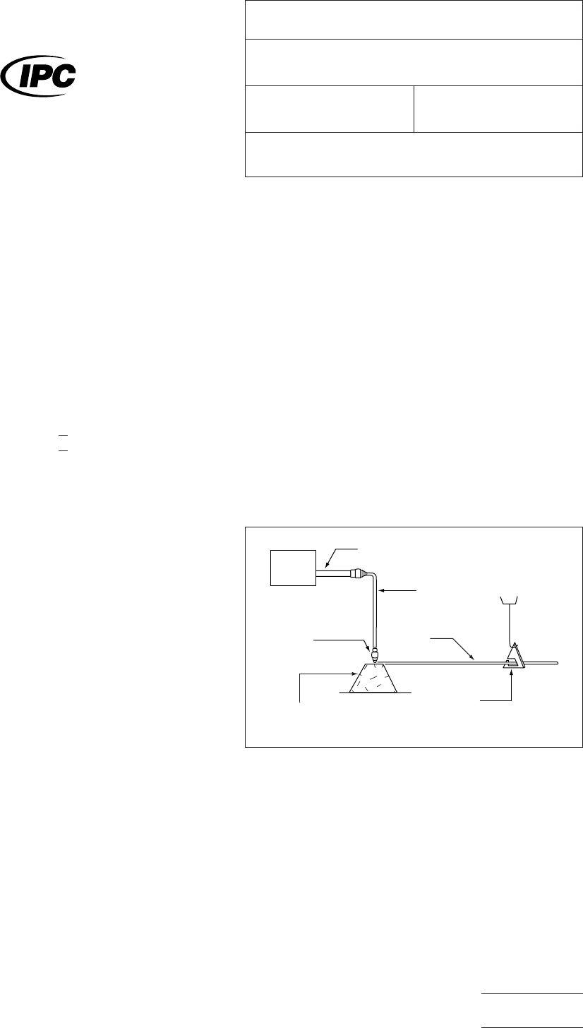
IPC-2-5-18-1
Figure
1 TDR Test Set-up for Measuring Characteristic
Impedance
TRD
Ref Z Airline
O
Hang
er
Test Cable
in Air
RG 58 C
Cable
Connection
Device
Non-Metallic
Surface
The
Institute for Interconnecting and Packaging Electronic Circuits
2215 Sanders Road • Northbrook, IL 60062
IPC-TM-650
TEST
METHODS MANUAL
Number
2.5.18
Subject
Characteristic
Impedance Flat Cables (Unbalanced)
Date
7/84
Revision
B
Originating Task Group
Material
in this Test Methods Manual was voluntarily established by Technical Committees of the IPC. This material is advisory only
and its use or adaptation is entirely voluntary. IPC disclaims all liability of any kind as to the use, application, or adaptation of this
material. Users are also wholly responsible for protecting themselves against all claims or liabilities for patent infringement.
Equipment referenced is for the convenience of the user and does not imply endorsement by the IPC.
P
age1of4
电子技术应用 www.ChinaAET.com