IPC-TM-650 EN 2022 试验方法.pdf - 第84页
1.0 Scope This method of test covers the procedure for determining the weights and/or thickness of etchable carrier copper foils for printed circuits. 2.0 Applicable Documents None. 3.0 Test Specimen Use template describ…

1.0
Scope
This
method of test covers the procedure for
determining the weight and/or thickness of releasable carrier
copper foils for printed circuits.
2.0
Applicable Documents
None.
3.0
Test Specimen
Use
template described below to cut
three samples of carrier copper foil. Samples should be taken
from near the left and right edges and center across the width
of the roll.
4.0
Apparatus
4.1
Balance
capable of weighing accuracy to ±0.001 grams.
4.2
Knife
suitable for cutting copper.
4.3
Template
pre-cut to 0.026 sq. meters [40 sq. in] 100
±0.1 mm by 250 ±0.1 mm [4 ±1/32 in by 10 ±1/32 in].
4.4
B-Stage
(prepreg) material and sufficient laboratory
equipment for lamination.
5.0
Procedure
5.1 Test
5.1.1
Cut
three specimens 100 x 250 mm [4 by 10 inches]
in size across the web of the roll.
5.1.2
Using
a balance, weigh three separate specimens to
the nearest 0.001 grams. Record the weights for each speci-
men.
5.1.3 Laminate
the three specimens to a B stage (prepreg)
material to a total thickness of 1 mm [0.062 in] thick (suggest
8 piles of No. 7628 glass style 0.17 mm [0.0068 in] nominal
thickness or equal).
5.1.4
After
lamination, remove the carrier substrate. Weigh
the carrier on a balance to the nearest 0.001 gram. Record
the weights, Subtract the weights recorded from the corre-
sponding weights in 5.1.2.
5.2
Evaluation
5.2.1
To
calculate the approximate thickness of the thin
copper foil in microns, multiply the weight difference obtained
in 5.1.4, by the factor 4.349.
5.2.2
To
calculate the area weight in grams per 6451 square
mm [254 square inches] of the carrier copper foil, multiply the
weight difference obtained in 5.1.4 by the factor 6.35.
5.2.3
To
calculate the area weight in ounces per 3657
square mm [square foot] of the carrier copper foil, multiply the
weight difference by the factor 0.127.
The
Institute for Interconnecting and Packaging Electronic Circuits
2215 Sanders Road • Northbrook, IL 60062
IPC-TM-650
TEST
METHODS MANUAL
Number
2.2.12.2
Subject
Weight
and Thickness of Copper Foils with
Releasable Carriers
Date
7/89
Revision
Originating Task Group
N/A
Material
in this Test Methods Manual was voluntarily established by Technical Committees of the IPC. This material is advisory only
and its use or adaptation is entirely voluntary. IPC disclaims all liability of any kind as to the use, application, or adaptation of this
material. Users are also wholly responsible for protecting themselves against all claims or liabilities for patent infringement.
Equipment referenced is for the convenience of the user and does not imply endorsement by the IPC.
P
age1of1
电子技术应用 www.ChinaAET.com

1.0
Scope
This
method of test covers the procedure for
determining the weights and/or thickness of etchable carrier
copper foils for printed circuits.
2.0
Applicable Documents
None.
3.0
Test Specimen
Use
template described below to cut
three samples of carrier copper foil. Samples should be taken
from near the left and right edges and center across the width
of the roll.
4.0
Apparatus
4.1
Balance
capable of weighing accuracy to ±0.001 grams.
4.2
Knife
suitable for cutting copper.
4.3
Template
pre-cut to 0.026 sq. meters [40 sq. in] 100
+0.1 mm by 250 ±0.1 mm [4 ±1/32 in by 10 ±1/32 in].
5.0
Procedure
5.1 Test
5.1.1
Cut
three specimens 100 x 250 mm [4 by 10 inches]
in size across the web of the roll.
5.1.2
Using
a balance, weigh three separate specimens to
the nearest 0.001 grams. Record the weights for each speci-
men.
5.1.3
Remove
the copper from the carrier substrate by
etching the samples in a 50% nitric acid solution for 30 sec-
onds or a suitable time to remove the copper foil. Rinse and
dry.
5.1.4
Reweigh
carrier substrate on the balance to the near-
est 0.001 gram. Record the weight of each sample. Subtract
the weights recorded from the corresponding weights in
5.1.2.
5.2
Calculation
5.2.1
To
calculate the approximate thickness of the etch-
able carrier copper foil in microns, multiply the weight differ-
ence obtained in 5.1.4, by the factor 4.349.
5.2.2
To
calculate the area weight in grams per 6451 square
mm [254 square inches], multiply the weight difference
obtained in 5.1.4 by the factor 6.35.
5.2.3
To
calculate the area weight of the etchable carrier in
ounces per 3657 square mm [square foot], multiply the weight
obtained in 5.1.4 by the factor 0.127.
The
Institute for Interconnecting and Packaging Electronic Circuits
2215 Sanders Road • Northbrook, IL 60062
IPC-TM-650
TEST
METHODS MANUAL
Number
2.2.12.3
Subject
Weight
and Thickness Determination of Copper
Foils with Etchable Carriers
Date
7/89
Revision
Originating Task Group
N/A
Material
in this Test Methods Manual was voluntarily established by Technical Committees of the IPC. This material is advisory only
and its use or adaptation is entirely voluntary. IPC disclaims all liability of any kind as to the use, application, or adaptation of this
material. Users are also wholly responsible for protecting themselves against all claims or liabilities for patent infringement.
Equipment referenced is for the convenience of the user and does not imply endorsement by the IPC.
P
age1of1
电子技术应用 www.ChinaAET.com
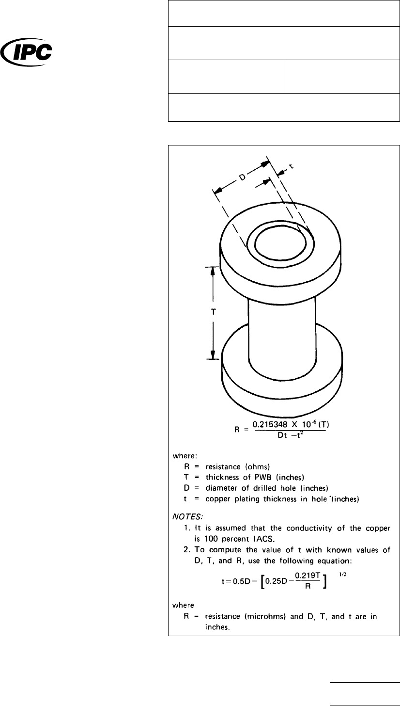
1.0
Scope
1.1
A
nondestructive inspection method for determining the
quality of plated-through connections in printed wiring boards.
1.2 Theory. Copper will display a resistivity of known value
depending upon the geometry of the shell and the conductiv-
ity of the copper. If the shell is not uniform, defects such as
cracks, voids, or thin spots in the copper will cause the mea-
sured resistance to be higher than the theoretical value. This
value is computed by using the equation given in Fig. 1.
2.0
Applicable Documents
IPC-TC-500
Specification
for copper plated through hole,
two-sided boards, rigid.
3.0
Test Specimen
3.1 Description of Specimens.
The
following types of
specimens can be tested using the equipment specified
herein:
(1) Printed wiring boards, either two-sided or multilayer,
which can fit properly within the neck of the test meter.
NOTE:
In
testing of plated-through holes in two-sided or
multilayer printed wiring boards, the measurement is the resis-
tance of the plating in the hole only and is not related to any
interconnected circuit terminating in that hole, unless there is
an electrically parallel circuit, i.e., two or more holes located
within 0.25″ of each other.
(2) Printed wiring boards up to 3/8’’ in thickness.
(3) Plated-through connections of any diameter which can
be spanned conveniently by the probes.
3.2
Specimen Preparation.
Insulating
materials such as
flux, conformal coatings, encapsulating compounds, adhe-
sives, mold release compounds, etc., shall be removed from
the terminal areas to allow a positive metal-to-metal contact to
be made between the probes and the plated-through hole
terminal area. Closely spaced conductors shall be masked to
prevent the probes from bridging between the terminal areas
and adjacent conductors. Whatever material is used to mask
the conductors shall be located in such a manner that the
probes are not separated from the hole to be measured.
Figure
1 Resistance Calculation of Plated-Through
Connection
The
Institute for Interconnecting and Packaging Electronic Circuits
2215 Sanders Road • Northbrook, IL 60062
IPC-TM-650
TEST
METHODS MANUAL
Number
2.2.13.1
Subject
Thickness,
Plating in Holes Microhm Method
Date
1/83
Revision
A
Originating Task Group
Printed Board Test Methods Task Group (7-11d)
Material
in this Test Methods Manual was voluntarily established by Technical Committees of the IPC. This material is advisory only
and its use or adaptation is entirely voluntary. IPC disclaims all liability of any kind as to the use, application, or adaptation of this
material. Users are also wholly responsible for protecting themselves against all claims or liabilities for patent infringement.
Equipment referenced is for the convenience of the user and does not imply endorsement by the IPC.
P
age1of4
电子技术应用 www.ChinaAET.com