IPC-TM-650 EN 2022 试验方法.pdf - 第749页
each approximately 0.7 in x 5 in. Layers 5 and 6 have no trace routing, so removing them provides an 8 layer coupon. Con- versely, by duplicating layers 5 and 6, a 14-layer or higher layer count coupon can be obtained. N…
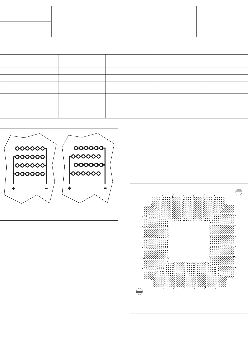
signal-2 vias; for a total of 168 potential in-line PTH-PTH fail-
ures for each spacing distance.
Holes Staggered (closest PTH-PTH spacing in diagonal direc-
tion): There are three rows of 26 signal-1 vias intermeshed
with four rows of 27 signal-2 vias; for a total of 312 potential
diagonal PTH-PTH failures for each spacing distance.
3.4 CAF Test Coupon/Board Quantity The CAF testing
data analysis technique recommended for either of these CAF
test coupon/board designs requires a minimum 25 CAF test
boards to be run per sample lot per bias level for statistical
significance. This provides a total of 4,200 potential in-line
hole-hole CAF failure sites and 7,800 potential diagonal hole-
hole CAF failure sites for each unique sample/condition set.
For comparison, on a 1,428 I/O BGA device (Figure 4) there
are about 500 power/ground pins. So with an average of
slightly less than two adjacent power/ground pin spacings per
pin there are about 1,000 potential in-line hole-hole CAF fail-
ure sites per BGA device. For a production board with the
equivalent of three of these BGA devices and about 1200
passives or other components with close power/ground pin
spacings, the total number of opportunities for in-line CAF fail-
ure would then be about 4,200 (about the same as the entire
CAF test board sample lot of 25 pieces).
3.5 CAF Test Small Coupon Designs The IPC-9255 and
IPC-9256 CAF test coupon designs (Figure 5) have 10 layers,
Table 2 Test Structures B1 through B4 Design Rules
B1 B2 B3 B4
Outer layer pad size 0.94 mm [0.0370 in] 0.89 mm [0.0350 in] 0.84 mm [0.0330 in] 0.75 mm [0.0300 in]
Inner layer pad size 0.94 mm [0.0370 in] 0.89 mm [0.0350 in] 0.84 mm [0.0331 in] 0.75 mm [0.0295 in]
Drilled hole size 0.81 mm [0.0319 in] 0.71 mm [0.0280 in] 0.57 mm [0.0224 in] 0.46 mm [0.0181 in]
Via edge to via edge
(shortest distance)
0.26 mm [0.0102 in] 0.37 mm [0.0146 in] 0.51 mm [0.0201 in] 0.62 mm [0.0244 in]
Via edge to via edge
(Manhattan Distance)
0.37 mm [0.0146 in] 0.52 mm [0.0205 in] 0.72 mm [0.0283 in] 0.88 mm [0.0346 in]
On IPC-9254 only, bias
applied between:
J7, J11 J8, J11 J9, J11 J10, J11
IPC-2625-3
Figure 3 CAF Test Board PTH-PTH Spacing Design
Staggered Hole to Hole (Section B)
In-Line Hole to Hole (Section A)
IPC-2625-4
Figure 4 BGA Device I/O Pin Assignment
928 Signal Pins
500 Power/ GND Pins
IPC-TM-650
Number
2.6.25
Subject
Conductive Anodic Filament (CAF) Resistance Test: X-Y Axis
Date
02/21
Revision
C
Page4of11
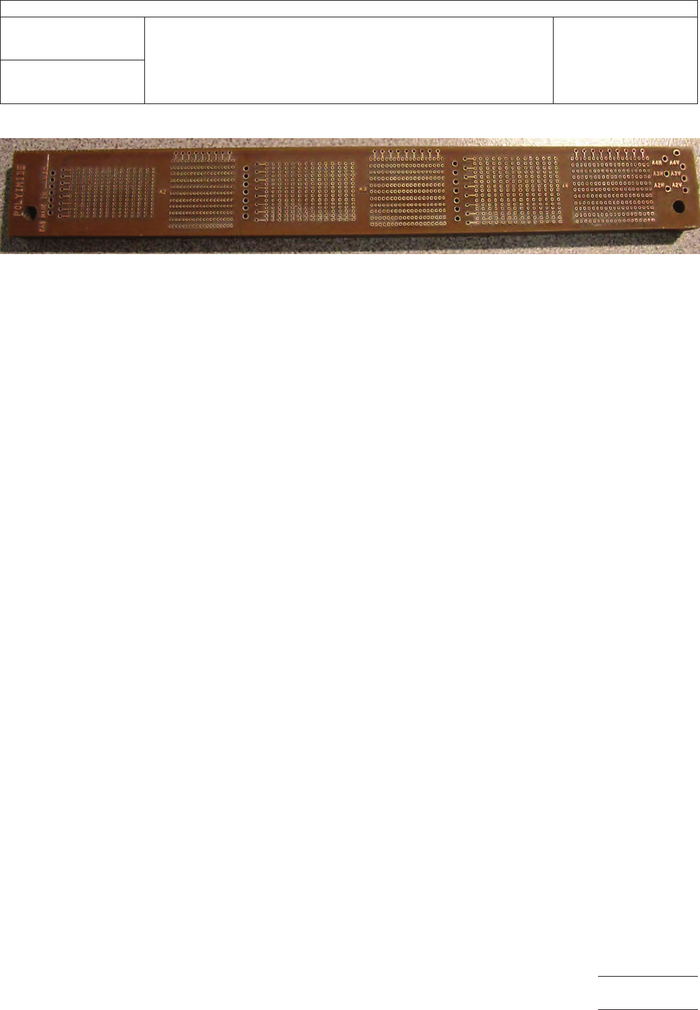
each approximately 0.7 in x 5 in. Layers 5 and 6 have no trace
routing, so removing them provides an 8 layer coupon. Con-
versely, by duplicating layers 5 and 6, a 14-layer or higher
layer count coupon can be obtained. Note: Inner layer copper
filling (similar to external layer copper thieving) can be applied
to inner layers. These two CAF test coupons have additional
features for identifying root cause failure site(s). Design data
should show the drill sizes to be used (example: 0.37 mm or
0.0145 in), but not the finished hole sizes after plating. Solder-
mask application is not required for these CAF test coupons.
• IPC-9256 CAF coupon evaluates the A2, A3 and A4 hole
wall to hole wall structures, with controlled spacings
between the adjacent plated through holes in both X and Y
in-line dimensions so good CAF test data is obtained even if
the laminate material machine direction lay-up is done incor-
rectly.
• IPC-9255 CAF coupon evaluates the A2, A3 hole wall to
hole wall structures, with controlled spacings between the
adjacent plated through holes in both X and Y in-line dimen-
sions (so good CAF test data is obtained even if the laminate
material machine direction lay-up is done incorrectly). This
coupon also evaluates the B2 structure where hole wall to
hole wall spacings are diagonal and useful for determining
the quality of the CAF testing performed (reference CAF test
method user guide).
[NOTE: These coupons can be run on production board lots
on unused portions of the working panel, allowing more cost-
effective on-going process and/or product monitoring of CAF
resistance.]
As a general rule, there should be enough CAF test boards
run within each sample test lot to have at least the equivalent
number of potential CAF failure sites as on a single targeted
specific application PWB.
4 Equipment/Apparatus or Material
4.1 Environmental Test Chamber
A clean test chamber
capable of producing and recording an environment of 65 ±
2°C[149±3.6°F]or85±2°C[185 ± 3.6 °F] and 87 +3/-2%
relative humidity, and that is equipped with cable access to
facilitate measurement cables to be attached to the speci-
mens under test.
4.2 Measuring Equipment A high resistance meter
equivalent to that described in ASTM D-257, with a range up
to 10
12
ohms and capable of yielding an accuracy of ± 5% at
10
10
ohms with an applied voltage of 100 ± 2 VDC, or an
ammeter capable of reading 10
-10
amps and capable of yield-
ing an accuracy of ± 5% in combination with 100±2VDC
power supply. The values of resistors used shall be verified
by reference resistors traceable to known industry or national
standards such as NIST.
4.3 Power Supply A power supply capable of producing a
standing bias potential of 10 VDC up to 100 VDC with a
tolerance of ± 2 VDC, and current supply capacity of at least
1 Ampere (Amp).
4.4 Current Limiting Resistors Tight control of the total
current limiting resistance value is critical for this test method.
One 10
6
ohm resistor in series shall be used for each current
path. Insert the current limiting resistors in series with the ter-
minating leads going to each test pattern. Note that some test
equipment has current limiting resistors built into the testing
systems. For the purposes of this standard test, excluding the
current limiting resistor and for each CAF test circuit, the total
series resistance of the measuring equipment and wires shall
not be more than 200 ohms. A lower total resistance value
will increase potential for damage to the test board when a
CAF failure occurs. A higher total current limiting resistance
value for each test net removes test conditions further from
actual field conditions and is not recommended.
4.5 Connecting Wire Use PTFE- or PFE-insulated copper
wires and solder the copper wire directly to the board to con-
nect test points for each test board to the measurement
apparatus. The insulation material should not outgas during
testing.
IPC-2625-3
Figure 5 Photo of CAF Test Coupon IPC-9256
IPC-TM-650
Number
2.6.25
Subject
Conductive Anodic Filament (CAF) Resistance Test: X-Y Axis
Date
02/21
Revision
C
Page5of11
4.6 Other Dedicated Fixtures Hard-wiring is the default
connection method. Other dedicated fixtures may be used,
provided that the fixture does not change the resistance by
more than 0.1 decade compared to a comparable hard-wired
system when measured at the test conditions. These fixtures
should be checked for their resistance values frequently.
5 Procedure
5.1 Test Specimen Preparation
5.1.1 Sample Identification
Use a method for identifying
each test board that does not cause contamination, such as
a scribe, making marks away from the biased area(s) of the
specimen. Test boards shall be handled by the edges of the
board only, and the use of noncontaminating gloves is recom-
mended. Each board shall be clearly marked to identify the
simulated assembly reflow and reword processing, and other
differentiating parameters, completed prior to CAF resistance
testing.
5.1.2 Prescreen for Opens and Shorts Perform
as-received insulation resistance measurements using a mul-
timeter to make connection to each net, and check for gross
defects. Check for shorts at a 1.0 megohm setting. No opens
are allowed in connected nets.
5.1.3 Simulated Assembly & Rework CAF test samples
shall go through representative assembly and rework thermal
cycling for the application. Default lead-free simulated assem-
bly and rework is 6X at 260 °C. Default simulated eutectic tin-
lead assembly and rework is 6X at 230 °C. For reference see
IPC-TM-650, 2.6.27 (method for assembly simulation).
5.1.4 Cleaning Entirely clean each sample (CAF test
board) per IPC-TM-650, Method 2.3.25, Detection and Mea-
surement of Ionizable Surface Contaminants by Resistivity of
Solvent Extract by immersion washing until the level of ionic
contamination is reduced to less than 1.0 microgram NaCl
equivalent per square centimeter and for a maximum of 20
minutes. Boards not achieving this level of cleanliness within
20 minutes shall be scrapped for the purposes of this test.
See IPC-TM-650, Method 2.6.27, Thermal Stress, Convection
Reflow Assembly Simulation.
5.1.5 Connecting Wire Plated through holes near one
edge of the board may be used for connecting wire to each
test circuit. The test board shall be covered with noncontami-
nating film to prevent flux spattering during the wire attach
process. After stripping back the wire insulation, use water
white rosin (per J-STD-004, Type B) and best soldering tech-
nique (per J-STD-001, Class 1 or 2) to solder (per J-STD-006,
Type Sn63) PTFE- or PFE-insulated wires to the connection
points on each test board. Ensure against damaging PWB
laminate material adjacent to the plated holes during soldering
by using appropriate time/temperature parameters for the sol-
dering iron.
5.1.6 Cleaning After Attachment Perform appropriate
local cleaning and rinsing after the attachment of the connect-
ing wires. Isolation resistance between connecting wire
attachment sites should remain excellent through 96 hours
conditioning. Note: Each CAF test failure that does occur dur-
ing subsequent testing should be checked to determine
whether the connecting wire attach area is the low resistance
site. If the connecting wire attach area rather than the daisy
chain area is the low insulation resistance site, then that test
sample is no longer valid for data analysis.
5.1.7 Dry Bake sample boards for a minimum of 30 min-
utes in a clean oven at 105±2°C[221.0 ± 3.6 °F].
5.1.8 Precondition Precondition test board samples in a
bias-free state (no electrical potential applied to any test pat-
tern) for 30 minutes minimum at 23±2°C[73.4 ± 3.6 °F] and
50 ± 5% relative humidity prior to any initial insulation resis-
tance measurements [measuring insulation resistance of each
daisy-chain net on each test board before starting the first 96
hours (± 30 minutes) of bias-free temperature and humidity
conditioning].
5.1.9 Temperature/Humidity/Bias ( T/H/B ) Chamber
Place the specimens in the environmental test chamber in a
vertical position such that the air flow is parallel to the direc-
tion of all test boards in the chamber. Allow at least approxi-
mately 2.5 cm [nominally 1.0 in] between each test board.
Place the test boards, as much as possible, toward the cen-
ter of the chamber to help ensure against nonoptimum air flow
and/or drops of condensation falling onto the test boards.
Dress all wiring away from the test patterns, keeping the wires
away from the test patterns as they are routed to the outside
of the chamber. Also, wire should not impede airflow around
the samples. Set the chamber temperature and humidity with
a ramp rate of one hour.
IPC-TM-650
Number
2.6.25
Subject
Conductive Anodic Filament (CAF) Resistance Test: X-Y Axis
Date
02/21
Revision
C
Page6of11