IPC-TM-650 EN 2022 试验方法.pdf - 第524页
B. Gore, J. Loyer, R. Mellitz, M. Gaudion, J. Burnikell, P. Carre, ‘‘Towards a PB Production Floor Metric for Go/No Go Testing of Lossy High Speed Transmission Lines,’’ from IPC Expo 2008. A. Deutsch, G. Arjavalingam, an…

The transmission line parameters R(f), L(f), C(f), and G(f) are a
consequence of determining α(f) and β(f) from the fitted trans-
mission line solution to the measurements. The final step is
the extraction of the relative dielectric constant ε
r
and loss
tangent, tanδ.
Measurements made of the capacitance and loss tangent of
an additional large parallel plate structure embedded in the
same layer with the signal conductor allows the extraction of
ε
r
and tanδ at very low frequencies. The final R(f), L(f), C(f), and
G(f) are used to extract the complex permittivity using Equa-
tions [1-2] and [1-3].
ε
r
(ω) =
(
C(ω)
C
1MHz
)
x ε
r1MHz
[1-2]
tanδ(ω) =
G(ω)
ωC(ω)
[1-3]
where C
1MHz
is the calculated line capacitance at a low
frequency such as 1 MHz and ε
r1MHz
is the value obtained at
1 MHz from the parallel plate measurement. ω is the angular
frequency and equal to 2πf.
The IPC SPP method is intended for printed boards, however
it can be extended to measure coaxial single-ended and dif-
ferential cables, flex cables, multi-chip module ceramic wiring,
single and multi-chip organic module wiring, thin-film wiring,
and on-chip wiring. The extraction results produce results in
frequency range between 10 KHz to 40 GHz, depending on
the quality of the TDR equipments and test coupon structure.
1.4 SET2DIL (Method D Description) In this method a
TDR step is injected into one half of a 101.6 mm [4.0 in] dif-
ferential pair, which has the two legs of the differential pair
shorted together at the far end. The waveforms of both halves
of the differential pair are captured and manipulated to derive
SDD21 (and Z
0
, if desired) of the equivalent differential pair.
1.4.1 SET2DIL Measurement System Caveats SET2DIL
produces the SDD21 value for the differential pair being mea-
sured; it is not intended to rigorously differentiate between
loss elements (conductor vs. dielectric, for instance). The
same structure can also be used to measure the differential
impedance, though that calculation isn’t covered in this speci-
fication. Some other limitations of SET2DIL include:
a) SET2DIL SDD21 measurements will include losses due to
the vias, for stripline traces. To minimize errors induced by
vias, the following limitations are made to the SET2DIL
coupon design:
i. The coupon has an effective length of 203.2 [8.0 in],
which will cause the trace losses to overwhelm small via
losses.
ii. Stripline traces on the bottom portion of the board
(lower layers) are measured from the top to minimize
via stub effects. Upper stripline layers are measured
from the bottom of the board.
b) SET2DIL SDD21 measurements will include an error term
from SDD11 effects if the differential trace being measured
isn’t 100 Ω (2x the reference impedance of 50 Ω).
i. The coupon has an effective length of 203.2 mm [8.0 in],
causing the trace insertion losses (SDD21) to overwhelm
the relatively small return loss.
ii. The primary purpose of SET2DIL is to ensure the trace
properties match that of those in simulations. Thus,
SDD21 from simulations with a 50 Ω reference can be
used as the measurement criteria for SET2DIL, making
the reference error difference moot.
1.5 FD (Method E Description) Three of the previously
described methods use TDR to determine the loss character-
istics of a printed board. This approach utilizes a Vector Net-
work Analyzer (VNA) or the fast fourier transform (FFT) of a
TDT for this purpose. The result is a direct measure of fre-
quency domain attenuation and loss. VNA equipment includes
calibration to the launch pad which must be used. The inser-
tion loss is directly related to transmission line design param-
eters utilized in signaling design analysis. The metric for the FD
method is the slope of the RMS insertion loss fit for a speci-
fied frequency range.
2 APPLICABLE DOCUMENTS
IPC-2141
Controlled Impedance Circuit Boards and High
Speed Logic Design
IPC-TM-650 Test Methods Manual
1.9 Measurement Precision Estimation for Variables Data
2.5.5.7 Characteristic Impedance of Lines on Printed Boards
by TDR
IEEE802.3ap Std 2007 Annex 69b.4.1, ‘‘Fitted attenuation’’
2.1 Technical Publications
R. Mellitz, T. Ballou, and S.G. Pytel, ‘‘Energy Based TDR Loss
Method for PB Manufacturers,’’ from IPCWorks 2005, Las
Vegas, NV.
IPC-TM-650
Number
2.5.5.12
Subject
Test Methods to Determine the Amount of Signal Loss on
Printed Boards
Date
07/12
Revision
A
Page3of24

B. Gore, J. Loyer, R. Mellitz, M. Gaudion, J. Burnikell, P.
Carre, ‘‘Towards a PB Production Floor Metric for Go/No Go
Testing of Lossy High Speed Transmission Lines,’’ from IPC
Expo 2008.
A. Deutsch, G. Arjavalingam, and G. Kopcsay, ‘‘Characteriza-
tion of Resistive Transmission Lines by Short Pulse Propaga-
tion,’’ in IEEE Microwave and Guided Wave Letters, vol. 2,
no.1, January 1992.
A. Deutsch, G. Arjavalingam, G. Kopcsay, and M. Deger-
strom, ‘‘Short-Pulse Propagation Technique for Characteriz-
ing Resistive Package Interconnections,’’ in IEEE Transactions
on Components, Hybrids, and Manufacturing Technology, vol.
15, no. 6, December 1992.
A. Deutsch, T. M. Winkel, G. Kopcsay, C. Surovic, B. Rubin,
G. Katopis, B. Chamberlin, R. Krabbenhoft, ‘‘Extraction of ε
r
(f)
and tanδ(f) for Printed Circuit Board Insulators Up to 30 GHz
Using the Short Pulse Propagation Technique’’ in IEEE Trans-
actions on Advanced Packaging, vol. 20, no. 1, February
2005.
A. Deutsch, C. W. Surovic, R. S. Krabbenhoft, G. V. Kopcsay,
B. J. Chamberlin, ‘‘Prediction of Losses Caused by Rough-
ness of Metallization in Printed-Circuit Boards,’’ IEEE Transac-
tions on Advanced Packaging, vol. 30, no.2, pp.279-287,
May 2007.
A. Deutsch, Roger Krabbenhoft, C. W. Surovic, B. Rubin,
T-M. Winkel, ‘‘Use of the SPP Technique to Account for Inho-
mogeneities in Differential Printed-Circuit-Board Wiring’’
Digest of SPI’08, Signal Propagation on Interconnects, May
12-15, Avignon, France, 2008 pp. 12-16.
G. Arjavalingam, A. Deutsch, G. V. Kopcsay, J. K. Tam,
‘‘Methods for the Measurement of the Frequency Dependent
Complex Propagation Matrix, Impedance Matrix, and Admit-
tance Matrix of Coupled Transmission Lines,’’ U.S. Patent,
patent 5,502,392, March 26, 1996.
J. Loyer, R. Kunze, ‘‘SET2DIL: Method to Derive Differential
Insertion Loss from Single-Ended TDR/TDT Measurements,’’
DesignCon 2010.
3 Test Coupons (Specimens)
3.1 Common Characteristics
The coupons for all the
methods contain transmission lines. The SPP coupon also
includes a small disc structure. The following are general
guidelines for designing transmission line test structures for
test methods within this document. These transmission line
test structures or interconnects may be placed within the
functional area of the printed board or within test coupons. A
coupon is a section of the printed board that is designated for
test structures and is removed from the panel after printed
board fabrication is completed. Differences between the char-
acteristics of test and functional interconnects may exist. The
relative merit of test structure placement relation to functional
circuit is beyond the scope of this document.
3.1.1 General Nomenclature – Coupons It is recom-
mended that coupons have labels that contain information
about the associated test line signal layer; for example, L1,
S3, etc. Labeling of the contact land for differential conductors
shall clearly indicate the matched pair.
It is recommended that test coupons include a printed board
serial number, part number, and date code.
3.1.2 Ground and Reference Planes All reference planes
in the coupon shall be connected together within the coupon
area and be independent of those planes in the functional cir-
cuit area. Ground and reference plane dispensation within the
functional area is beyond the scope of this document.
3.1.3 Differential Coupons The differential line is also
known as a balanced transmission line. The probing area
should contain four contact lands: one contact land for each
of the two signal conductors in the differential pair and two
contact lands connected to the reference plane(s).
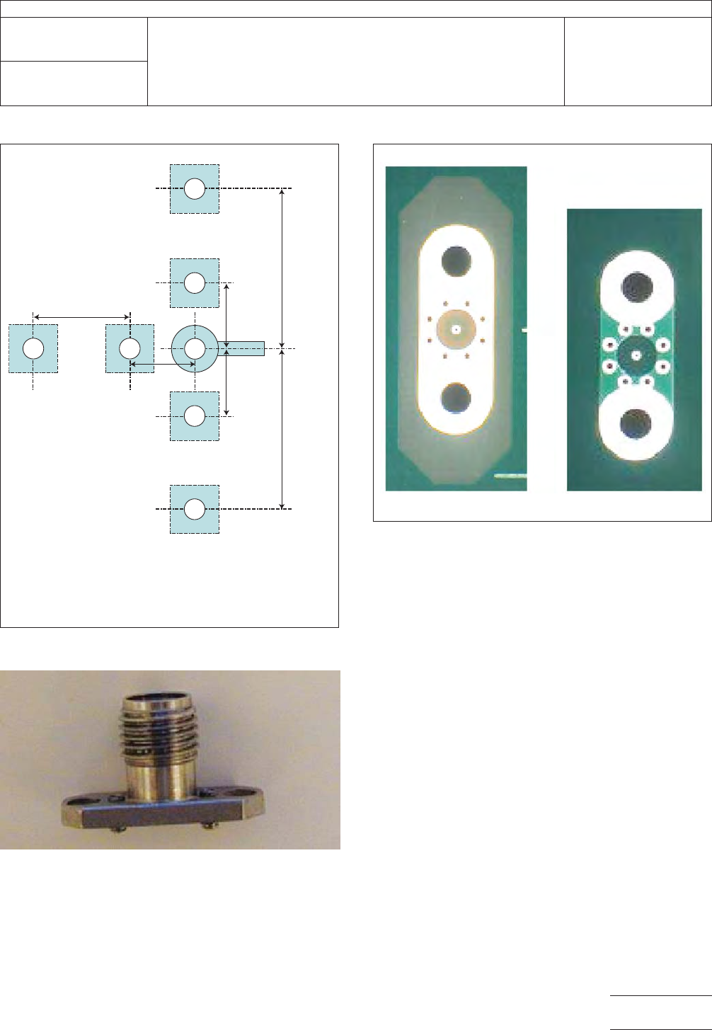
3.1.4 Probe Launch The probe launch is comprised of a
PTH or other via structure and ground contact rectangular
pad and an example is depicted in Figure 3-1. The hole diam-
eter is recommended to be the smallest hole that is appropri-
ate for the respective technology. Some printed boards may
employ blind and buried vias. The recommended pitch
between ground and signal pad for high volume testing is
1.016 mm [0.040 in] or 2.54 mm [0.100 in]. Higher accuracy
can be achieved with smaller ground pad to signal pad spac-
ing and use of multiple ground vias.
3.1.5 Connector Launch A high bandwidth connector
launch may be used instead of probe launch as show in Fig-
ure 3-2.
Figure 3-3 provides an example of high bandwidth connector
launch.
3.1.6 General Surface Condition The panel test coupons
shall have the same surface plating and use the same solder
mask requirements as the functional printed board.
IPC-TM-650
Number
2.5.5.12
Subject
Test Methods to Determine the Amount of Signal Loss on
Printed Boards
Date
07/12
Revision
A
Page4of24
3.1.7 General Thieving Thieving which is the use of
nonterminated copper structures, such as planes, pads,
and/or conductors adjacent to test lines that ensure plating
consistency may be used on test coupon. All thieving struc-
tures, if used, shall be placed at least six times the width of
the signal conductor (of the test interconnect) or 2.5 mm
[0.100 in], whichever is greater, from each test interconnect.
3.1.8 Termination Types of Test Lines There are two
types of line styles that may be used. The first is terminated on
each end with a launch. These lines are the only type that are
employed with the SPP and VNA method. The second type of
line is terminated on one end with a launch while the other end
is just the end of a conductor e.g., unterminated. The EBW
and RIE method may use either terminated or unterminated
lines types. The SET2DIL structure requires no termination.
3.1.9 Test Line Routing The test lines shall be routed
over/under contiguous ground/voltage planes. The test line
conductors shall be kept at least six times the height of the
laminate layer thickness which is closest to the conductor or
2.54 mm [0.100 in], whichever is greater; from printed board
structures include voids, plane splits, other conductors, and
holes.
It is recommended that test lines be straight.
3.1.10 Environmental Conditioning: Temperature and
Humidity
Temperature and humidity effect loss measure-
ments. Consistent results can be obtained by storing test
IPC-25512-3-1
Figure 3-1 Example of Probe Launches
Ground Rectangles: 0.572 mm [0.0225 in] square
Signal Pad: 22.5 mil 0.572 mm [0.0225 in] diameter
Hole Diameter: smallest hole for respective PCB technology
2.54 mm
[0.100 in]
2.54 mm
[0.100 in]
2.54 mm
[0.100 in]
1.016 mm
[0.040 in]
1.016 mm
[0.040 in]
1.016 mm
[0.040 in]
Figure 3-2 High Bandwidth SMA Connector Example
IPC-25512-3-3
Figure 3-3 High Bandwidth Connector Launch Example
IPC-TM-650
Number
2.5.5.12
Subject
Test Methods to Determine the Amount of Signal Loss on
Printed Boards
Date
07/12
Revision
A
Page5of24