IPC-TM-650 EN 2022 试验方法.pdf - 第508页
interconnects, but a practical issue of operator ability to use hand-held probes may be considered. Test reports must report any deviation from the nominal contact land and PTH geometry. 3.9 Contact Land Pitch Whenever p…
3) Outside of the PB area and at the center or edge of the
panel.
If coupons are placed in all the locations listed above, a com-
parison between a statistically significant sample set taken
from each location over time can yield data that will relax
placement requirements without reducing confidence in test
results.
3.5 Test Interconnect Geometry The test structures
should use the same line width and conductor thickness, and
be located in the same dielectric environment (permittivity,
thickness, and layering) as the target functional interconnects.
Spacing between conductors should also match that of the
functional interconnects. If edge coupons are used, and pre-
vious studies have shown that conductors at the edge of the
panel experience different lamination from those in functional
panel areas, then a compensation factor may be needed to
adjust the propagation delay measurement for this difference.
3.6 Lengths for Two-Line Test Structure When using
two nonfunctional transmission lines as the test structures,
thenominal physical lengths of the transmission line pair
should be 76.2 mm [3.0 in] and 152.4 mm [6.0 in]. Variations
in test structure lengths shall be documented.
3.7 Transmission Line Termination Transmission lines
are to be terminated at both ends using PTHs to allow electri-
cal connections to both ends of the line. Additionally, PTH ter-
minations at both ends provide for DC and low frequency
measurements of resistance, capacitance, conductance, and
inductance as additional diagnostic tools in the event of an
out-of-specification condition.
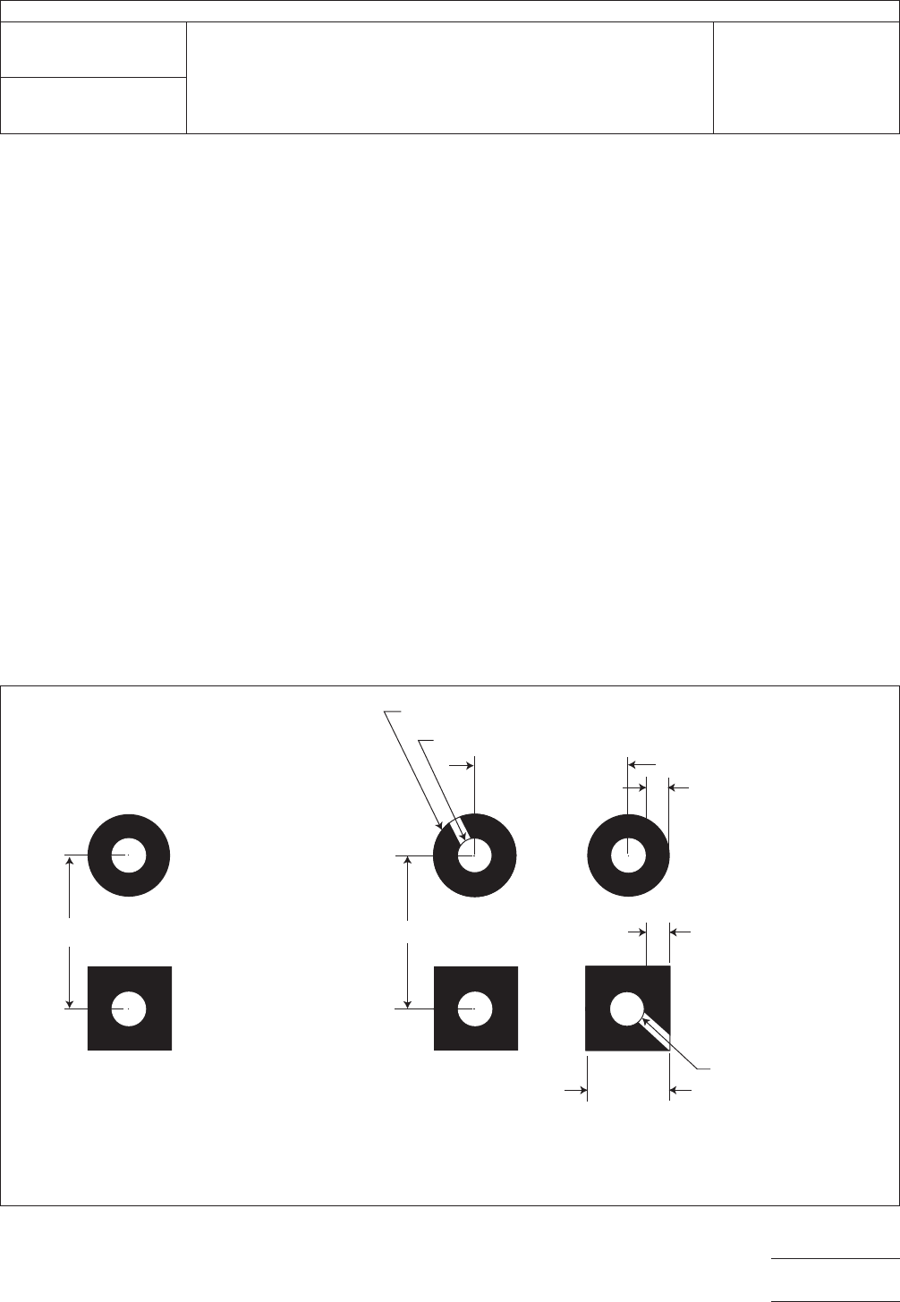
3.8 Contact Land The contact land should comprise PTHs
and contact pads as shown in Figure 3-1. Reference contact
lands should be square to aid in visual identification. The
nominal hole diameter shall be 0.46 mm [0.018 in] and sur-
face land shall be 1.02 mm [0.040 in]. However, the PTH
should be of consistent dimensions to ensure repeatability
and reliability of the tests for the given measurement equip-
ment. Care must be used when specifying different hole sizes
and land pitches since their electrical properties may affect the
reported t
D
in a secondary manner. Hole size should be larger
only if required by plating/aspect ratio requirements. Ideally,
hole and pad size should be the same as those of functional
IPC-25511-3-1
Figure 3-1 Contact Lands
1.91 mm [0.075 in]
1.91 mm [0.075 in]
1.02 mm [0.040 in]
0.46 mm [0.018 in]
0.28 mm [0.011 in]
0.28 mm [0.011 in]
1.91 mm [0.075 in]
ø0.46 mm [0.018 in]
ø1.02 mm [0.040 in]
SINGLE-ENDED
(1.91 mm [0.075 in])
DIFFERENTIAL
(1.91 mm [0.075 in] SQUARE)
SIGNAL LANDS
REFERENCE
LANDS
IPC-TM-650
Number
2.5.5.11
Subject
Propagation Delay of Lines on Printed Boards by TDR
Date
04/2009
Revision
Page3of16
interconnects, but a practical issue of operator ability to use
hand-held probes may be considered. Test reports must
report any deviation from the nominal contact land and PTH
geometry.
3.9 Contact Land Pitch Whenever possible, the center-
to-center distance between the signal and reference lands
of the test interconnect should be consistent to simplify
probing requirements and ensure measurement repeatability
and reproducibility. Nominal center-to-center pitch shall be
1.91 mm [0.075 in]. The use of different contact and probe
pitches must be specified and documented.
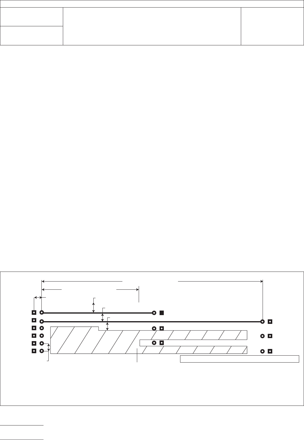
3.10 Single-Signal Conductor Transmission Line The
single-signal conductor transmission line is also known as the
single-ended, unbalanced, and asymmetrical structure. The
probing area for these lines should consist of a contact land
(see Figure 3-2) for each signal line. The contact land should
provide connection to the reference, or ground, connection for
the test structure. This method requires the use of one con-
tact pitch to ensure measurement consistency between the
test structures of the specimen.
3.11 Orientation The contact land orientation (placement
and angle of the contact land of the signal line relative to the
contact land of the reference plane) must be the same for all
test interconnects of the specimen in order to ensure mea-
surement consistency between test interconnects.
3.12 Test Interconnect Routing
a. The test interconnects shall only be routed over and under
contiguous ground and voltage planes following controlled
line impedance guidelines (see IPC-2141). The test inter-
connects must not extend into PTH clearance areas.
b. The test interconnects shall be kept at least six times the
width of the signal conductor or 2.5 mm [0.0984 in],
whichever is greater, from any PTHs and any other inter-
connect on the same plane. All conductive material (such
as copper nomenclature, copper thieving, etc.) shall be
kept at least 2.5 mm [0.0984 in] from each test intercon-
nect.
c. Test interconnects shall be straight or contain gradual and
rounded bends.
3.13 Nomenclature Labeling of all test interconnect con-
tact lands on at least one surface layer is required for opera-
tor identification during manual probing operations. The label
shall minimally contain information about which signal layer
the test interconnect is modeling (for example, L1-3in, L1-6in,
etc.). Nomenclature should be etched in copper and be
spaced a minimum of at least six times the width of the signal
conductor (of the test interconnect) or 2.5 mm [0.0984 in],
whichever is greater, from the test interconnect area. When-
ever practical, the terminations at both ends of test intercon-
nect shall be marked.
IPC-25511-3-2
Figure 3-2 Transmission Line Structures
2.54 mm
[0.100 in] MIN
2.54 mm [0.100in] MIN
2.54 mm [0.100 in] MIN
1.91 mm [0.075 in]
152.4 mm [6.00 in] REF
76.2 mm [3.00 in] REF
1.91 mm [0.075 in]
L1/3.0 Layer One – 3 Inch Line
L1/6.0 Layer One – 6 Inch Line
L3/3.0 Layer Three – 3 Inch Line
L3/6.0 Layer Three – 6 Inch Line
L1/3.0
L1/6.0
L3/3.0
L3/6.0
L7/3.0
L7/6.0
THIEVING
NOTES:
PN#. LOT#.
SN#.
IPC-TM-650
Number
2.5.5.11
Subject
Propagation Delay of Lines on Printed Boards by TDR
Date
04/2009
Revision
Page4of16
3.14 Additional Guidelines for Testing Panel Coupons
Test interconnects may be contained within one or more
panel coupons. It is recommended that there be at least one
coupon per PB on the panel as long as it does not adversely
affect panel utilization. With this configuration, the following
additional design guidelines apply. More than one coupon
may be necessary on a PB to ensure uniformity. Also, more
test interconnects may be required than can fit inside one test
coupon. In that case, more than one test coupon is neces-
sary.
3.14.1 Reference and Ground Planes All reference
planes existing in the coupon are to be connected together
within the coupon area and be electrically independent of con-
ductor planes in the functional circuit area.
3.14.2 Surface Condition The panel test coupons shall
have the same surface plating and use the same solder mask
requirements as the functional PB.
3.14.3 Thieving Differences in circuit density between the
inside of a panel coupon and the functional area may produce
surface plating and etching differences. In order to compen-
sate for these differences, thieving (the use of nonterminated
copper structures, such as planes, pads, and/or traces adja-
cent to test lines) may be used. All thieving structures shall be
kept at least six times the width of the signal conductor (of the
test interconnect) or 2.5 mm [0.0984 in], whichever is greater,
from each test interconnect.
4 Apparatus and Instrumentation The TDR measure-
ment system contains a step generator, a high-speed sam-
pling oscilloscope, and all the necessary accessories for con-
necting the TDR unit to the test structures under test. IPC-
2141 provides a discussion of the TDR system architecture,
system considerations, and the TDR measurement processes
used herein.
4.1 Measurement System Requirements
4.1.1 Voltage Measurement Accuracy
The voltage mea-
surement accuracy and linearity of the TDR sampling oscillo-
scope shall be sufficient to provide the required accuracy in
the value of propagation delay. Nominally, the voltage mea-
surement accuracy should be better than ± 1%.
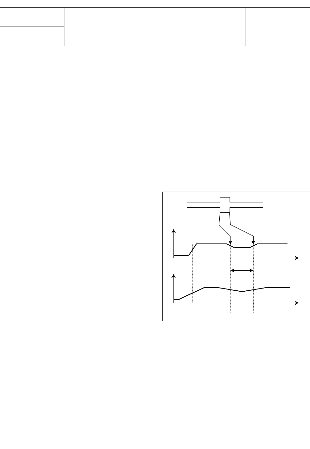
4.1.2 Temporal/Spatial Resolution The resolution limit of
a given TDR unit is defined as that particular time or distance
wherein two discontinuities or changes on the transmission
line being measured, that would normally be individually dis-
cernable, begin to merge together because of limited TDR
system bandwidth, timing jitter, or a reduced signal-to-noise
ratio. The resolution limit is specified in either time or distance,
and is always related to the one-way propagation time
between the two discontinuities t
P
(see Figure 4-1), and not
the round trip propagation time 2 t
P
.
Per this definition, the temporal resolution limit is:
a. one half of the system risetime, that is 0.5 t
sys
, where t
sys
is the 10 to 90% risetime or 90% to 10% falltime depend-
ing on the propagating edge of the TDR signal;
and the spatial resolution limit is:
b. 0.5 t
sys
xv
p
, where v
p
is the signal propagation velocity in
the transmission line being measured.
For a given length of transmission line to be measured, the
resulting spatial resolution of the TDR measurement set-up
should not exceed one fourth (0.25) of the available length of
the transmission line L
TL
. In other words, L
TL
should be at
least four times the spatial resolution of the measurement sys-
tem.
Table 4-I relates TDR system risetime values to minimum
L
TL
for typical surface microstrip lines in air on FR4 PB mate-
rial (v
p
≈ 2x10
8
m/s).
IPC-25511-4-1
Figure 4-1 Resolution and Electrical Length of
Transmission Line
t
V
transmission line
adequate resolution
inadequate resolution
t
V
2 t
p
IPC-TM-650
Number
2.5.5.11
Subject
Propagation Delay of Lines on Printed Boards by TDR
Date
04/2009
Revision
Page5of16