IPC-TM-650 EN 2022 试验方法.pdf - 第583页
current preset on the Hipot test instrument, causing the instrument to indicate a failure when in fact there was none. The charging current of the capacitor is affected by the change in voltage from one ramp step to anot…

3.3 Test Specimen Conditioning All qualification test
specimens shall be conditioned at 23 °C±3°Cand50%±
10% RH for 24 hours, before testing. For conformance test-
ing, such conditioning is optional.
4 Apparatus
4.1 Hipot Test Instrument
A Hipot test instrument is a
piece of equipment capable of supplying a range of DC test
voltages appropriate for the materials under test with adjust-
able ramp rate and hold-time settings. The Hipot equipment
shall have an adjustable threshold current setting. (see 5.2.4)
The user shall ensure that the Hipot test instrument satisfies
the original manufacturer’s technical specifications.
4.2 High Voltage Connections Contacts (conductor
plates) apply the voltage from the Hipot test instrument to the
test specimen’s Top Imaged Foil and Bottom Foil (see Figure
1). These contacts should not contain sharp points that could
damage either the copper foil or the dielectric layers of the test
specimens.
CAUTION: Dangerous voltages may be present on the test
connections. Use proper machine guarding and/or machine
interlocking.
5 Procedure
5.1
This test method shall be performed on fresh test
specimens. Hipot testing shall not be conducted on test
specimens that have previously been exposed to high voltage
levels or other similar testing.
NOTE: Some dielectrics may show acceptable Hipot results
(i.e., ‘‘Pass’’) after defects have been ‘‘burned out’’ at high
voltage (see Section 6).
5.2 Program the Hipot test instrument with the appropriate
peak voltage, voltage ramp rate, hold time at peak voltage
and current threshold level. These values shall be recorded.
5.2.1 The peak voltage should be as specified in the mate-
rial Specification Sheet (see IPC- 4821) under the parameter
‘‘Hipot (Volts DC).’’
5.2.2 For qualification testing, the voltage ramp rate shall
be 5% of the peak voltage per second, unless otherwise
specified. For conformance testing, the voltage ramp rate
shall be 5% of the peak voltage per second or AABUS.
5.2.3 For qualification testing, the hold time at peak voltage
shall be 30 seconds +3 / -0 seconds. For conformance test-
ing, the hold time at peak voltage shall be a minimum of 10
seconds or AABUS.
5.2.4 The threshold settings shall be set to a value greater
than the in-rush current (due to the charging of the test speci-
men) observed when the voltage is increased (see 6.1). Many
commercial Hipot test instruments display the current during
the test. The in-rush current can be determined by setting the
threshold current to a high value and then observing the cur-
rent spikes as the voltage is ramped to the peak voltage. After
several test specimens have been tested and the currents
observed, set the threshold current to be greater than the
highest current observed. For example, if the in-rush current is
20 microamperes and the current at peak voltage is 1 micro-
ampere, set the threshold current to 40 microamperes.
5.3 The test specimen shall be placed between the con-
tacts of the Hipot test equipment (see Figure 1). Start the
Hipot sequence.
5.4 Upon completion of the test, the Hipot sequence should
include the discharge of the test specimen.
SAFETY NOTE: Larger test specimens, with high capaci-
tance density, may take more time than expected to dis-
charge.
5.5 Reporting The Hipot test instrument indicates either
Pass or Fail of the material under test. A current surge above
the threshold current setting indicates a Failure. This includes
very short term current surges or ‘‘arcs’’ that occur due to the
burnout of defects. Such unacceptable current surges may
also be the result of dielectric failure or manufacturing defects.
For qualification testing, if the test specimen Passes, record
the leakage current per unit area and the passing voltage. If
the qualification test specimen Fails, record the failure voltage
and threshold current per unit area of each test specimen.
For conformance testing, reporting requirements should be
AABUS.
6 Notes
6.1
When the Hipot test instrument voltage changes from
one level to the next higher level during the ramp-up to the
final voltage, the in-rush current will initially surge above the
steady state current because the capacitor is charging. It is
possible that this surge in current could exceed the threshold
IPC-TM-650
Number
2.5.7.2
Subject
Dielectric Withstanding Voltage (Hipot Method) - Thin Dielectric
Layers for Printed Boards
Date
11/2009
Revision
A
Page2of3

current preset on the Hipot test instrument, causing the
instrument to indicate a failure when in fact there was none.
The charging current of the capacitor is affected by the
change in voltage from one ramp step to another, the dielec-
tric constant of the dielectric, the thickness of the dielectric
and the area of the capacitor. High dielectric constant, very
thin dielectric thickness and large area of the capacitor plates
will all cause the charging current to increase. As a result, the
threshold current setting on the Hipot test instrument may
need to be adjusted to avoid generating a false failure condi-
tion.
6.2 Some thin and filled dielectrics will require a higher
threshold current setting, compared to unfilled materials. This
is particularly true of dielectrics containing ferroelectric com-
pounds, such as barium titanate. These materials may show
a nonlinear response between current and voltage. This is not
an issue at most operating voltages, which are normally low,
but can be an issue for the Hipot test. At high voltage levels,
these materials may trigger a false failure because they allow
more current than the threshold setting.
6.3 Materials, especially very thin and/or highly filled materi-
als, may have a leakage current per unit area that is area
dependent when tested at the specified test voltage. Thus,
results from the qualification test specimen or other small area
test structures may not reflect the actual leakage current per
unit area when the material is tested in a significantly larger
area format, such as that commonly done in conformance
testing by a material supplier.
6.4 Reference Documents
ASTM D149
‘‘Dielectric Breakdown Voltage of Solid Electri-
cal Insulating Materials at Commercial Power Frequencies’’
IPC-TM-650
Number
2.5.7.2
Subject
Dielectric Withstanding Voltage (Hipot Method) - Thin Dielectric
Layers for Printed Boards
Date
11/2009
Revision
A
Page3of3
1
Scope
The
purpose of this test method is to quickly
assess the adequacy of a given Anisotropically Conductive
Adhesive Film (ACF) construction and bonding process for
avoiding short circuits between adjacent traces of a flex circuit
being bonded to a low profile circuit substrate.
1.1
Purpose
ACF
materials are often used to interconnect
fine-pitch flexible circuitry to substrates such as flat-panel dis-
plays. A center to center pitch range of 80 µm to 200 µm is
not uncommon in circuits for flat panel display applications. It
is critical that the particle dispersion within the ACF be of suf-
ficient quality such that there is no inherent tendency for short
circuits between adjacent traces. In addition, it is important
that a bonding process is used, which doesn’t create any
undue accumulation of particles, which will lead to short cir-
cuits.
2
Applicable Documents
None
3
Test Specimens
3.1
In
order to perform this test, a custom-designed and
fabricated flex circuit substrate will need to be produced.
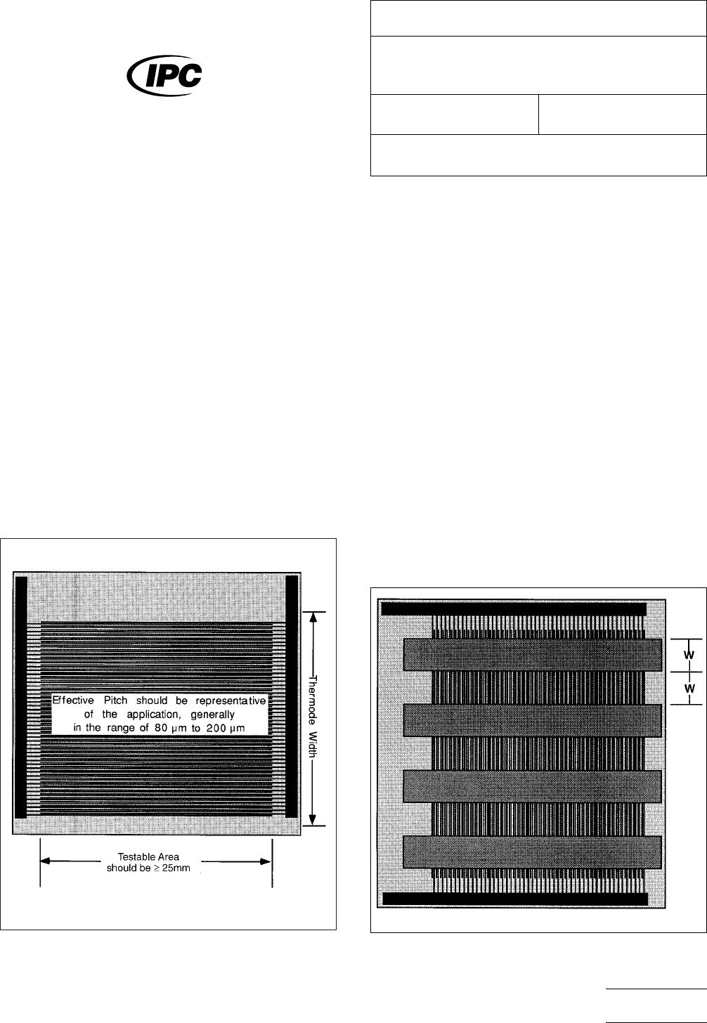
A suggested flex circuit construction of a design is shown in
Figure 1. Flex circuit materials should be selected to be repre-
sentative of what is being used in the application. The traces
alternate between anodic and cathodic polarity as shown.
Trace thickness, width, and pitch, should be selected in
accordance with the application. Total trace count should be
at least 100, and total width of the pattern should be slightly
less than the thermode length. Total length of the traces
should be sufficient to allow at least four bonds to be accom-
modated as shown in Figure 2 and Figure 3.
N is the number of circuit traces (at least 100).
I is the measured leakage current in amps after 10 seconds @
50V.
g is the gap spacing between adjacent traces on the circuit in
mm (of the order 0.04 mm to 0.1 mm).
IPC-2-5-10-1-1
Figure
1 Suggested Flex Circuit Layout for Insulation
Resistance Test
IPC-2-5-10-1-2
Figure
2 Preattachment of the ACF Strips to the Flex
Circuit
The
Institute for Interconnecting and Packaging Electronic Circuits
2215 Sanders Road • Northbrook, IL 60062
IPC-TM-650
TEST
METHODS MANUAL
Number
2.5.10.1
Subject
Insulation
Resistivity for Adhesive Interconnection
Bonds
Date
11/98
Revision
Originating Task Group
SMT Mounting Adhesives Task Group (5-24d)
Material
in this Test Methods Manual was voluntarily established by Technical Committees of the IPC. This material is advisory only
and its use or adaptation is entirely voluntary. IPC disclaims all liability of any kind as to the use, application, or adaptation of this
material. Users are also wholly responsible for protecting themselves against all claims or liabilities for patent infringement.
Equipment referenced is for the convenience of the user and does not imply endorsement by the IPC.
P
age1of2
电子技术应用 www.ChinaAET.com