IPC-TM-650 EN 2022 试验方法.pdf - 第678页
When used for qualification purposes, the base laminate will be FR-4 epoxy-glass with 17 µm [0.5 oz equivalent] unpro- tected copper metalization. 4 Apparatus 4.1 A clean test chamber capable of producing and record- ing…
1
Scope
This
test method is used to characterize the
effects of flux residues on electrical performance by determin-
ing the degradation of electrical insulation resistance under
conditions of high temperature and humidity.
This method, in conjunction with the supporting documenta-
tion in IPC-J-STD-004, is intended to be equivalent to Telcor-
dia Technologies GR-78-CORE, Section 13.1, (Corrosiveness
of Soldering Fluxes) and is used primarily by telecommunica-
tions companies to qualify the candidate flux or solder paste.
2
Applicable Documents
IPC-J-STD-004
Requirements
for Soldering Fluxes
IPC-A-600
Acceptability
of Printed Board
GR-78-CORE
Physical
Design and Manufacture of Telecom-
munications Product - Telcordia Technologies (Formerly
Bellcore)
ASTM
D-257
Standard
Test Methods for DC Resistance or
Conductance of Insulating Materials
2.1
Master Drawings
Telcordia
Technologies Test Pattern (GR-78-CORE, Figures
14.1 and 14.2)
IPC-A-25A
Multipurpose
1-sided Test Pattern
IPC-A-50
Surface
Insulation Resistance Phoenix Board
3
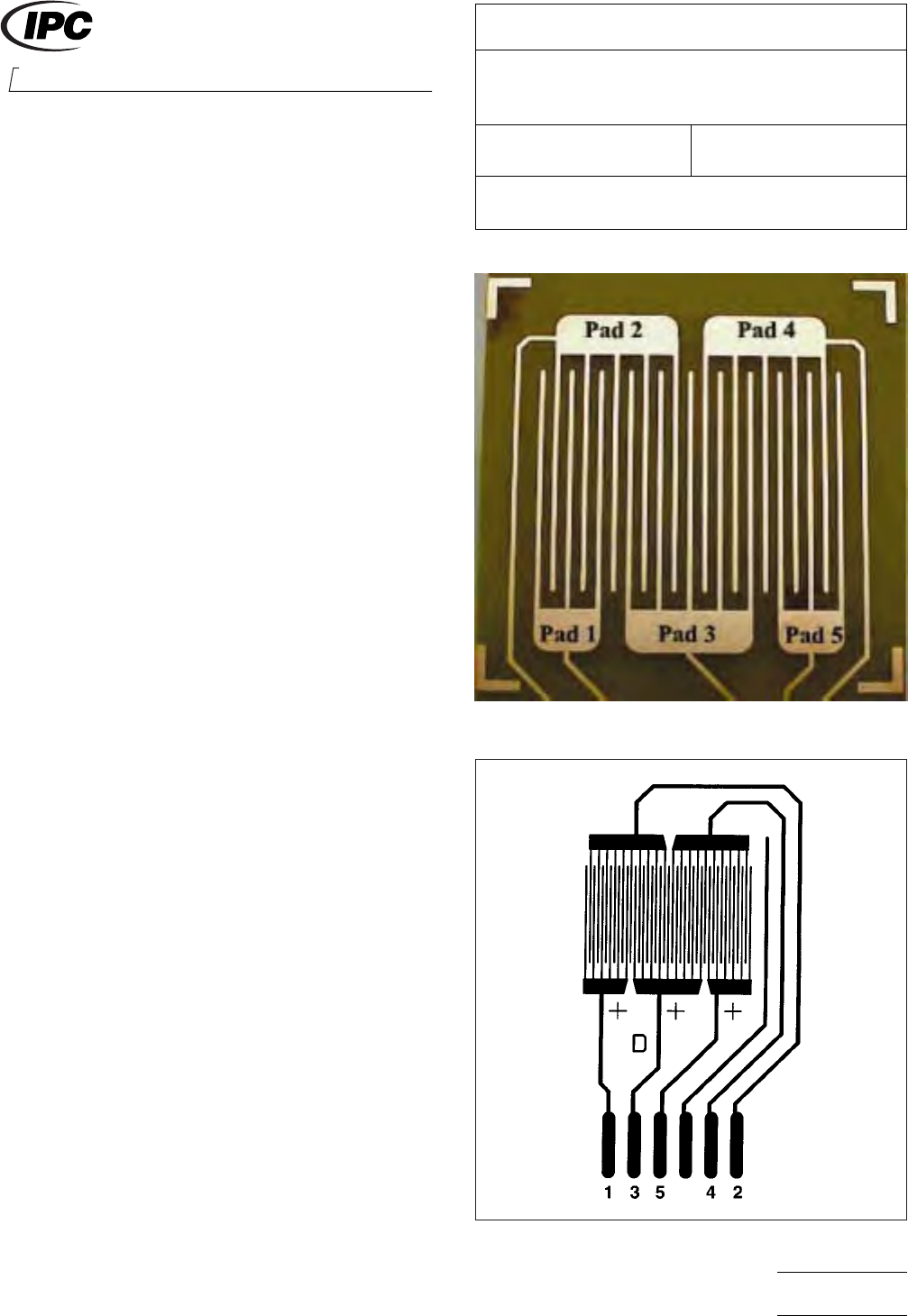
Test Specimens
The
test specimens for this test method
may be either of the interdigitated comb pattern shown in Fig-
ures1or2.
These test patterns can be produced in a number of formats.
Both of these patterns can be found on the IPC-B-50 Stan-
dard Test Board. The pattern shown in Figure 2 can be found
on the IPC-B-25A test board (pattern D). Artwork for manu-
facturing these boards is available through the master draw-
ings listed in 2.1. Contact IPC for a listing of vendors provid-
ing prefabricated test boards.
The comb pattern in Figure 1 has 0.65 mm [0.025 in] lines and
1.27 mm [0.050 in] spacings. This test pattern is also com-
monly referred to as the Bellcore pattern.
The comb pattern in Figure 2 has 0.32 mm [0.0125 in] lines
and spaces (see Note 6.4).
Figure
1
IPC-2636-2
Figure
2
2215
Sanders Road
Northbrook, IL 60062-6135
IPC-TM-650
TEST
METHODS MANUAL
Number
2.6.3.6
Subject
Surface
Insulation Resistance - Fluxes -
Telecommunications
Date
01/04
Revision
Originating Task Group
Surface Insulation Resistance Task Group, 5-32b
Material
in this Test Methods Manual was voluntarily established by Technical Committees of IPC. This material is advisory only
and its use or adaptation is entirely voluntary. IPC disclaims all liability of any kind as to the use, application, or adaptation of this
material. Users are also wholly responsible for protecting themselves against all claims or liabilities for patent infringement.
Equipment referenced is for the convenience of the user and does not imply endorsement by IPC.
P
age1of3
ASSOCIA
TION CONNECTING
ELECTRONICS INDUSTRIES
®
电子技术应用 www.ChinaAET.com

When
used for qualification purposes, the base laminate will
be FR-4 epoxy-glass with 17 µm [0.5 oz equivalent] unpro-
tected copper metalization.
4
Apparatus
4.1
A
clean test chamber capable of producing and record-
ing an environment of 35°C ± 2°C [95°F ± 3.6°F] and 88%
-0+5% relative humidity, and that allows the insulation resis-
tance of the patterns to be measured under these conditions.
The chamber must be capable of maintaining these conditions
under load (i.e., with specimens in place).
4.2 Measuring
equipment such as that described in ASTM
D-257 with a range up to 10
13
ohm
and capable of yielding an
accuracy of ± 5% at 10
12
ohm
and an applied potential of 100
Vdc.
5
Test
5.1 Sample Sizes
•
Three test patterns are produced for test with no applied
solder mask and no applied flux (controls).
• Three test patterns are produced for test using the candi-
date material(s) and process(s).
• Sample preparation and enumeration shall also be in accor-
dance with IPC-J-STD-004 ‘‘SIR samples for Flux Qualifica-
tion.’’
5.2
Sample Identification
Use
a non-contamination
method for identifying the test sample (e.g., vibrating scribe).
During this process, handle the samples by the edges only or
using non-contaminating gloves.
5.3
Wire Attach
Cover
the test patterns with non-
contaminating film, such as aluminum foil or plastic film, to
prevent flux spattering during the wire attach process. Use
water white rosin (non-activated flux) or dry-solder (no flux at
all) to solder PTFE-insulated wires to the connection points of
the specimens. Do not attempt to remove the flux residues.
Alternatively, connections may be made by mechanical pres-
sure connections (e.g., alligator clips).
NOTE: Because of the very high resistance levels typically
used as pass-fail criteria for this method, a connector-based
or other fixtured setup is not recommended, due to leakage
currents, unless these systems can be shown to have no sig-
nal degradation compared to hardwiring.
It is an option to pre-condition test samples for 24 hours at 23
°C [73 °F] and 50% R.H. before testing.
5.4
Placing in Chamber
Place
the specimens in the envi-
ronmental chamber in a vertical position such that the airflow
is parallel to the direction of the board in the chamber. Allow
at least 1.25 cm [0.5 in] between each test sample. Dress all
wiring away from the test patterns. Route the wires to the
outside of the chamber. Set the chamber temperature to
35°C [95°F] and 85% minimum relative humidity, with a ramp
time of not less than one hour. There is no electrical potential
applied to any test pattern during the first 24 hours of test
exposure.
5.5
Resistance Measurements
After
24 hours of test
exposure with no applied electrical potential, measure the
insulation resistance of each pattern using an applied voltage
of 100 ± 2 volts DC and an electrification time of 60 seconds.
NOTE: It is recommended that the temperature and humidity
levels be verified to be within the recommended limits prior to
beginning the resistance measurements.
Each comb pattern requires four test measurements. Mea-
surements are made between (see Figure 1):
• Pad 1 to Pad 2
• Pad 3 to Pad 2
• Pad 3 to Pad 4
• Pad 5 to Pad 4
Pads 2 and 4 are at one potential and Pads 1, 3, and 5 are at
ground potential (see Note 6.3).
Determine the means of the dataset as outlined in 5.6.
After the 24 hour measurements, apply a bias of 48 volts DC
to all test patterns, using the same polarity as used for the
resistance measurements.
After an additional 72 hours (96 hours total), repeat the mea-
surement series using an applied voltage opposite in polarity
to that of the conditioning bias.
Remove all bias from the test specimens and return the cham-
ber to ambient conditions over a one hour period. Remove all
samples from the chamber for visual examination.
5.6
Data Analysis
The
average insulation resistance for
each sample group, taken at 24 hours and again at 96 hours,
shall be greater than the minimum set forth in IPC-J-STD-004.
The average insulation resistant (IR
avg
)
shall be defined as the
IPC-TM-650
Number
2.6.3.6
Subject
Surface
Insulation Resistance - Fluxes - Telecommunications
Date
01/04
Revision
P
age2of3
电子技术应用 www.ChinaAET.com
geometric
mean of the sample set and can be calculated from
the following:
IR
avg
= 10
[
1
N
Σ
1
N
log
10
(IR)
i
]
Where:
N
= Number of Test Points (12 nominal for each set of three
patterns).
IR
i
=
individual insulation resistance measurements (see 6.6
for an example).
No individual insulation resistance value may be more than a
factor of 10 below the specified minimum value.
Where an assignable cause of low insulation resistance, which
is properly attributable to the laminate itself, or to the process
used to produce the PCB, can be found, then such a value
can be excluded from calculating the average value, provided
that at least 10 (of the original 12) test points are included in
the average.
Such assignable causes include the following:
• Contamination on the insulating surface of the board, such
as lint, solder splines or water droplets from the chamber.
• Incompletely etched patterns that decrease the insulating
space between the conductors by more than the amount
allowed in the appropriate design requirements drawing.
• Scratched, cracked, or obviously damaged insulation
between conductors.
5.7
Visual Analysis
Discoloration
of the patterns (green,
blue-green, blue, or blue-black coloration of the conductors)
shall be considered a failure.
6
Notes
6.1
If
condensation occurs on the test specimens in the
environmental chamber while the samples are under voltage,
dendritic growth will occur. This can be caused by a lack of
sufficient control of the humidification of the oven. Water spot-
ting may also be observed in some ovens where the airflow in
the chamber is from back to front. In this case, water conden-
sation on the cooler oven window can be blown around the
oven as micro-droplets which deposit on test specimens and
cause dendritic growth if the spots bridge the distance
between two electrified conductors. Both of these conditions
must be eliminated for proper testing.
6.2 Tight
control of the test humidity is critical for this test
method. A difference of 5% relative humidity can result in a
0.5 - 1.0 decade difference in the measured resistance. . The
uniformity of the environment is also important. A fully loaded
chamber, where airflow is severely impeded, may have a
30-40% RH range within the chamber workspace.
6.3
The
polarity of the applied voltage is not important as
long as the application is consistent (e.g., Pads 1, 3, 5 are
positive and 2, 4 are at ground potential, vs. Pads 2 and 4
positive, and Pads 1, 3, 5 at ground potential).
6.4
The
0.318 mm [0.0125 in] lines/space pattern can also
be found on the obsolete IPC-B-25 standard test board. This
board was re-designed for improved SIR measurement accu-
racy (better routing of traces) and carries the designation IPC-
B-25A. Pattern D of the B-25A board is preferred over the B/E
pattern of the IPC-B-25.
6.5
IR
ave
is
also referred to as the geometric mean of the
data set. Most spreadsheet packages contain functions for
calculating the geometric mean of a data set. If you are com-
puting the geometric mean of a large dataset, the spread-
sheet may come back with an error because the number is so
large. In such cases, use the antilog of the LogOhm average
to arrive at the geometric mean. See the following example.
6.6
Example of Numerical Calculations
Three
5-point test patterns (4 measurements each)
LogOhms = base-10 logarithm of measured resistance
Average of LogOhms = 11.84
Antilog of LogOhm Average = 6.94E+11 ohms =
Geometric Mean = IR
ave
No.
Resistance (Ohms) LogOhms
1
3.98E+11 11.60
2 1.58E+11 11.20
3 6.31E+11 11.80
4 7.94E+11 11.90
5 1.00E+12 12.00
6 1.00E+12 12.00
7 3.98E+11 11.60
8 1.58E+12 12.20
9 1.26E+12 12.10
10 1.26E+12 12.10
11 1.00E+12 12.00
12 3.98E+11 11.60
IPC-TM-650
Number
2.6.3.6
Subject
Surface
Insulation Resistance - Fluxes - Telecommunications
Date
01/04
Revision
P
age3of3
电子技术应用 www.ChinaAET.com