IPC-TM-650 EN 2022 试验方法.pdf - 第717页
separate measurements are needed to obtain a statistically meaningful result. 6.0 PWB Process Test/Sampling For testing of lot con- formity at least ten different PWBs with parallel conductors as per Section 3 shall be t…
1.0
Scope
This
test method will demonstrate a relative
degree to which uncoated printed wiring boards are suscep-
tible to dendritic growth due to the presence of ionic residues
and condensed moisture. This test method is particularly suit-
able for printed wiring board manufacturing process control.
2.0
Applicable Documents
IPC-TR-476
How
to Avoid Metallic Growth Problems on
Electronic Hardware
MIL-P-551
10
Printed
Wiring Boards
3.0
Test Specimens
Test
pattern is chosen from, but not
restricted to e.g., MIL-P-55110 type ‘‘Y’’ pattern with a pair of
conductors having typically 15-30 mils separation (See Figure
1). A pair of parallel conductors on an uncoated production
printed wiring board, with spacing between conductors of
approximately 15-30 mils is suitable as well.
4.0
Equipment/Apparatus
4.1 Power Supply
A
dc power supply capable of providing
a metered 0-20 V dc, and 100 milliamps current.
4.2
Microscope
50-100
power microscope and means of
providing direct and/or indirect lighting on specimen.
4.3
Miscellaneous Items
DI
water sample (2 oz.) kept in a
plastic bottle, eye dropper, a 1/2 watt-10K ohm current limit-
ing resistor and a stop watch.
5.0
Procedure
5.1 Preparation
5.1.1
Attach
a wire to each of the conductors on the ‘‘Y’’
pattern test board, or to corresponding, parallel conductors
on a production PWB.
5.1.2
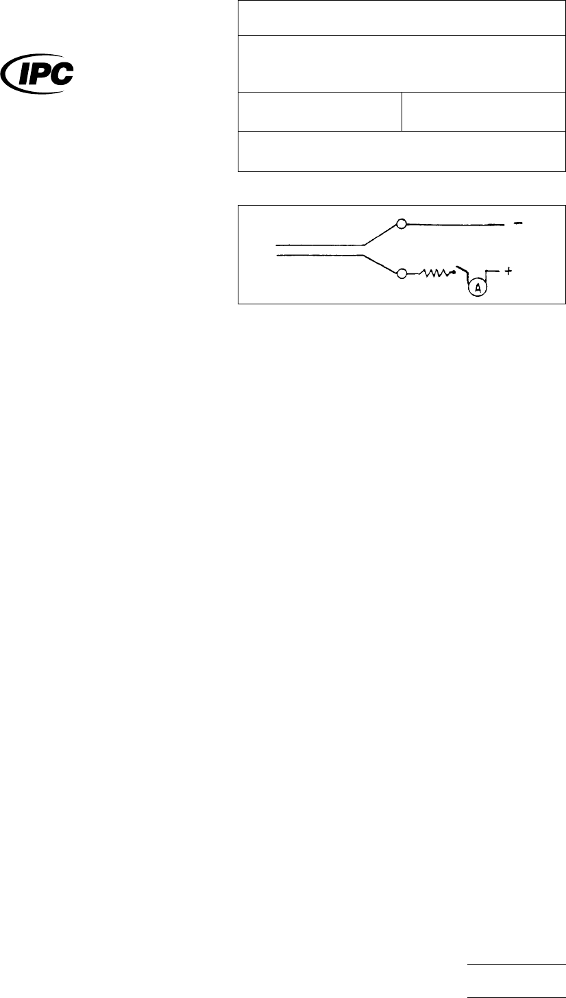
Connect
a 10K resistor in series to the power supply
as shown in Figure 1. The resistor will limit the current to 1.5
milliamp maximum.
5.1.3 Place
the board for viewing on the microscope, so
that the parallel conductors are in view. Provide lighting that
will illuminate the test board on top and/or underneath.
5.1.4
Using
the eye dropper, place a drop of DI water
across the conductors that are in view under the microscope,
at least 0.5 inch away from the place where external wires are
attached to parallel conductors. Adjust power supply to 15 V
and turn the power supply on. Simultaneously start the stop-
watch.
5.1.5
Carefully
observe the action using the microscope.
Adjust the power of the microscope so the entire water area
is in view.
5.1.6 Bubbles
may appear within about 5 seconds. This is
hydrogen evolution-electrolysis of water.
5.1.7 Depending
on PWB ionic cleanliness level and the
characteristics of the PWB surface, there may be a dendritic
(tree-like) growth from the negative to positive conductor,
appearing within a typical (for a given board) but generally very
broad time span of a few seconds to several minutes.
5.1.8
The
condition of dendritic growth is much easier to
observe with an artificial light source placed under the test
board. A clear demonstration of the dendritic growth can be
performed if tap water containing ionic contamination is used
in place of DI water (see paragraph 5.1.4).
5.1.9
Once
the dendritic growth has reached the positively
charged conductor, most action will cease; turn off the stop-
watch. The elapsed time is a relative measure of susceptibility
of the PWB in question to undergo dendritic growth under
high humidity (condensed moisture) environment. At least ten
IPC-2613-1
Figure
1
The
Institute for Interconnecting and Packaging Electronic Circuits
2215 Sanders Road • Northbrook, IL 60062-6135
IPC-TM-650
TEST
METHODS MANUAL
Number
2.6.13
Subject
Assessment
of Susceptibility to Metallic Dendritic
Growth: Uncoated Printed Wiring
Date
10/85
Revision
Originating Task Group
N/A
Material
in this Test Methods Manual was voluntarily established by Technical Committees of the IPC. This material is advisory only
and its use or adaptation is entirely voluntary. IPC disclaims all liability of any kind as to the use, application, or adaptation of this
material. Users are also wholly responsible for protecting themselves against all claims or liabilities for patent infringement.
Equipment referenced is for the convenience of the user and does not imply endorsement by the IPC.
P
age1of2
电子技术应用 www.ChinaAET.com

separate
measurements are needed to obtain a statistically
meaningful result.
6.0
PWB Process Test/Sampling
For testing of lot con-
formity at least ten different PWBs with parallel conductors as
per Section 3 shall be tested.
7.0
Test Interpretation
Test
for susceptibility to metallic
dendritic growth is a relative measure of localized ionic residue
levels. As such, it does not have direct relationship with abso-
lute PWB reliability measure. The results of this test are found
useful in the PWB process control by testing board-to-board
and lot-to-lot variations.
IPC-TM-650
Number
2.6.13
Subject
Assessment
of Susceptibility to Metallic Dendritic Growth:
Uncoated Printed Wiring
Date
10/85
Revision
P
age2of2
电子技术应用 www.ChinaAET.com
1 Scope This test method is used to determine the ability of
a polymer solder mask protective coating to withstand an
environment conducive to electrochemical migration.
2 Applicable Documents
IPC-A-25A-G-KIT
1
Multipurpose One-Sided Test Pattern -
Gerber Format
IPC-SM-840 Qualification and Performance of Permanent
Solder Mask
IPC-TR-476 Electrochemical Migration: Electrically Induced
Failures in Printed Wiring Assemblies
J-STD-004 Requirements for Soldering Fluxes
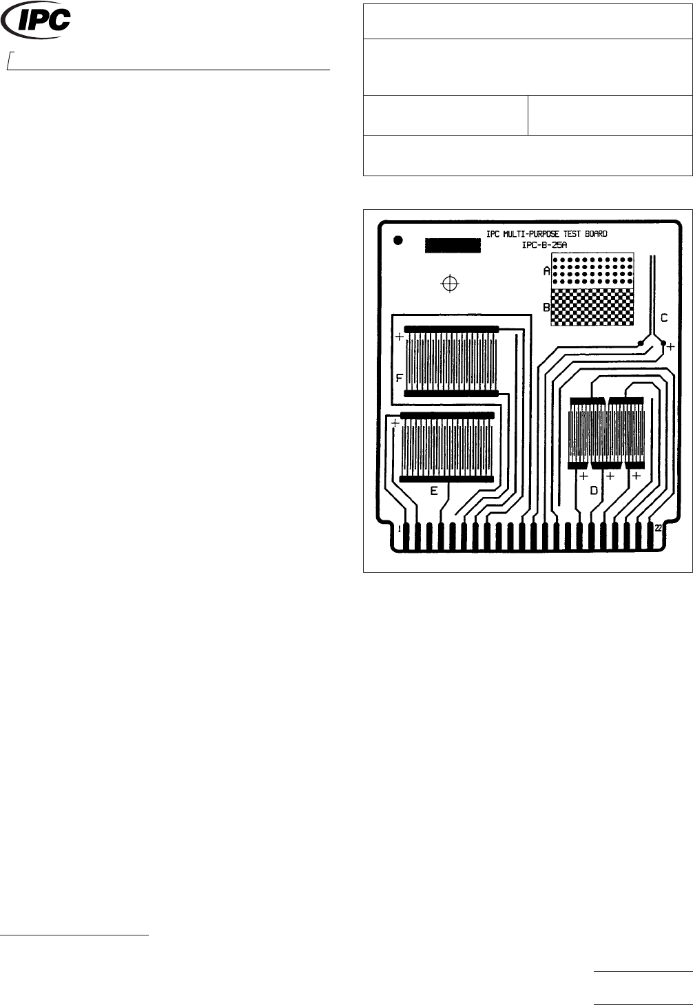
3 Test Specimens The IPC-A-25A-G-KIT artwork package
provides the Gerber files necessary for the fabrication of the
standard IPC-B-25A test board used with this test method.
3.1 Qualification Testing Three IPC-B-25A boards (see
Figure 1) using the D comb patterns with 0.32 mm [0.0126 in]
lines and spaces for both Classes T and H, coated with sol-
der mask according to the solder mask supplier’s recommen-
dations.
3.2 Conformance Testing Three IPC-B-25A boards (see
Figure 1) using the C comb pattern (‘‘Y’’ shape pattern) which
should be 0.64 mm lines/0.64 mm spacing [0.025 in lines/
0.025 in spacing] or the pattern with the minimum spacing on
the production board, whichever has the smallest line spac-
ing, coated with solder mask according to the solder mask
supplier’s recommendations.
4 Equipment/Apparatus
4.1 Power Supply
Capable of supplying 10 ± 0.5 VDC at
1 A, maximum.
4.2 Oven Capable of maintaining up to 90±1°C[194 ±
1.8 °F].
4.3 Chamber Capable of maintaining 85±2°C[185 ± 3.6
°F] with 85%, minimum, relative humidity.
4.4 Desiccator 25 cm [9.84 in] diameter minimum, with
openings for the connecting wires to pass through while main-
taining a hermetic seal.
4.5 Potassium Sulfate Reagent Grade potassium sulfate.
4.6 RTV Dow Corning 732 RTV potting compound or
equivalent.
4.7 Resistors 10 megohm resistor for Class H testing and
1 megohm resistors for Class T testing
4.8 Magnifier Capable of supplying 10X magnification
4.9 Soldering Iron
1. www.ipc.org/onlinestore
IPC-2614-1
Figure 1 IPC-B-25A Test Board
3000 Lakeside Drive, Suite 309S
Bannockburn, IL 60015-1249
IPC-TM-650
TEST METHODS MANUAL
Number
2.6.14
Subject
Solder Mask - Resistance to Electrochemical
Migration
Date
03/07
Revision
D
Originating Task Group
Solder Mask Performance Task Group (5-33b)
Material in this Test Methods Manual was voluntarily established by Technical Committees of IPC. This material is advisory only
and its use or adaptation is entirely voluntary. IPC disclaims all liability of any kind as to the use, application, or adaptation of this
material. Users are also wholly responsible for protecting themselves against all claims or liabilities for patent infringement.
Equipment referenced is for the convenience of the user and does not imply endorsement by IPC.
Page1of4
ASSOCIATION CONNECTING
ELECTRONICS INDUSTRIES
®