IPC-TM-650 EN 2022 试验方法.pdf - 第617页
5.1.2 Choose configuration and strip wires out one 2.5 cm on each end (for testing stacked configuration, prepare two identical samples). 5.2 Interlayer Crosstalk 5.2.1 Clamp the cable in brackets so that it is suspended…
1
Scope
This
test method gives a procedure to determine
crosstalk or the magnitude of disturbance that is coupled to
one conductor when another conductor in a given cable con-
figuration is activated with a pulse.
2
Applicable Documents
None
3
Test Specimen
3.1
3.1
m ± 6.4 m length of cable
4
Equipment/Apparatus
4.1
Fast
rise pulse generator
4.2
Sampling
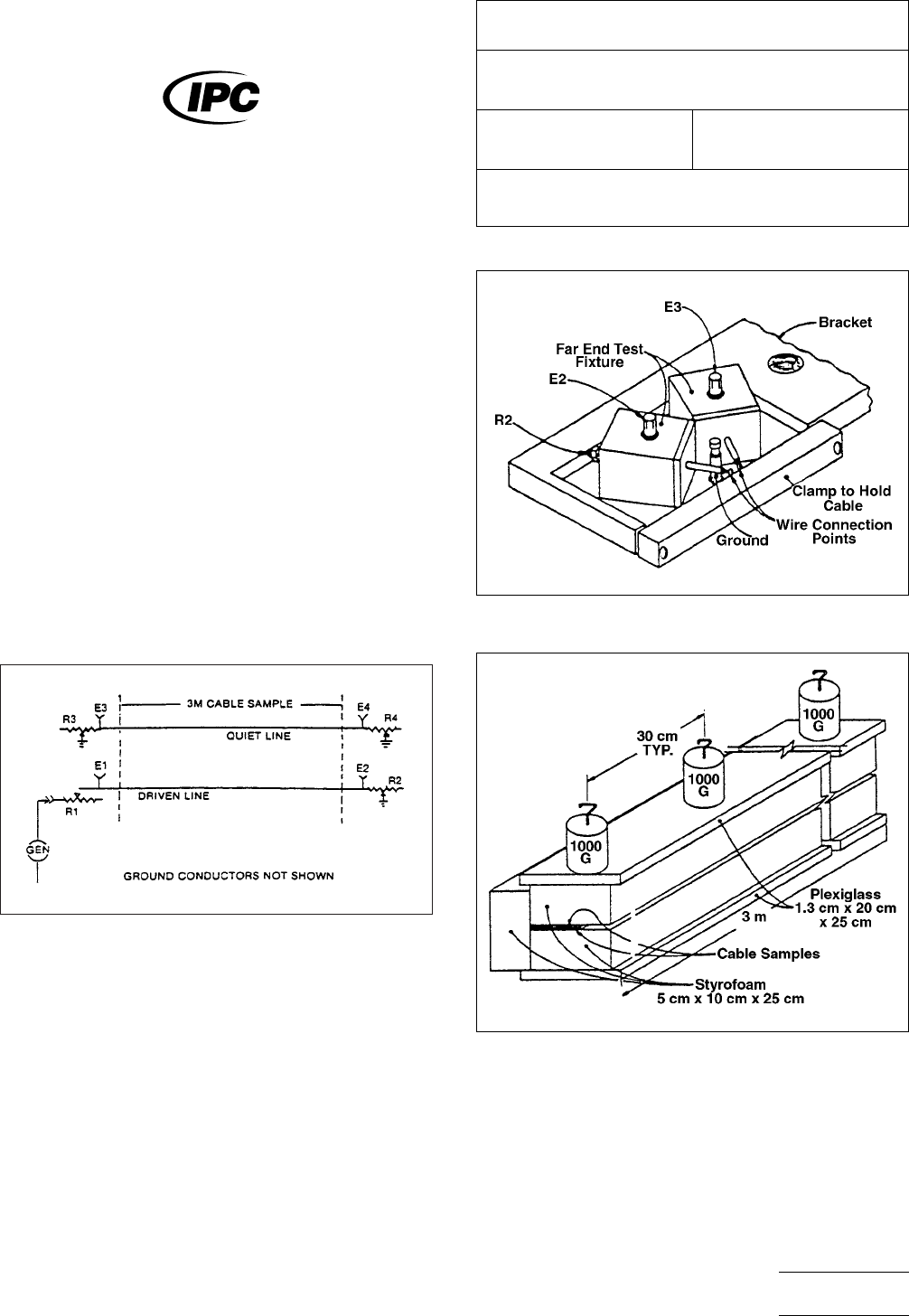
plug-in in appropriate oscilloscope (see Figure
1) with a high input impedance probe (≥152 m)
4.3
Test
fixture to introduce signal, provide oscilloscope
pickoff points, impedance matching and terminating potenti-
ometers, and a means of connecting sample (see Figure 2)
4.4 Brackets
to hold cable suspended in air and support fix-
ture close to end of cable system
4.5
Styrofoam
with rigid backing for ‘‘stacked’’ crosstalk
(see Figure 3)
4.6
Ohmmeter
5
Procedure
5.1 Setup
5.1.1
Set
pulse generator as follows:
Rep Rate ........................................................... 1 megahertz
Pulse Amp .......................................................... 2 to 5 volts
Pulse Width .................................................... 1 nanosecond
Rise Time .................................................... 2.5 nanosecond
IPC-2-5-21-1
Figure
1 Oscilloscope
IPC-2-5-21-2
Figure
2 Connecting Sample
IPC-2-5-21-4
Figure
3 Crosstalk
The
Institute for Interconnecting and Packaging Electronic Circuits
2215 Sanders Road • Northbrook, IL 60062
IPC-TM-650
TEST
METHODS MANUAL
Number
2.5.21
Subject
Digital
Unbalanced Crosstalk, Flat Cable
Date
3/84
Revision
A
Originating Task Group
Material
in this Test Methods Manual was voluntarily established by Technical Committees of the IPC. This material is advisory only
and its use or adaptation is entirely voluntary. IPC disclaims all liability of any kind as to the use, application, or adaptation of this
material. Users are also wholly responsible for protecting themselves against all claims or liabilities for patent infringement.
Equipment referenced is for the convenience of the user and does not imply endorsement by the IPC.
P
age1of2
电子技术应用 www.ChinaAET.com
5.1.2
Choose
configuration and strip wires out one 2.5 cm
on each end (for testing stacked configuration, prepare two
identical samples).
5.2
Interlayer Crosstalk
5.2.1
Clamp
the cable in brackets so that it is suspended in
air away from any conductive surface.
5.2.2
Connect
the wires to appropriate terminals on the test
fixture, taking care to keep lead lengths as short and neatly
dressed as possible without shorting.
5.2.3
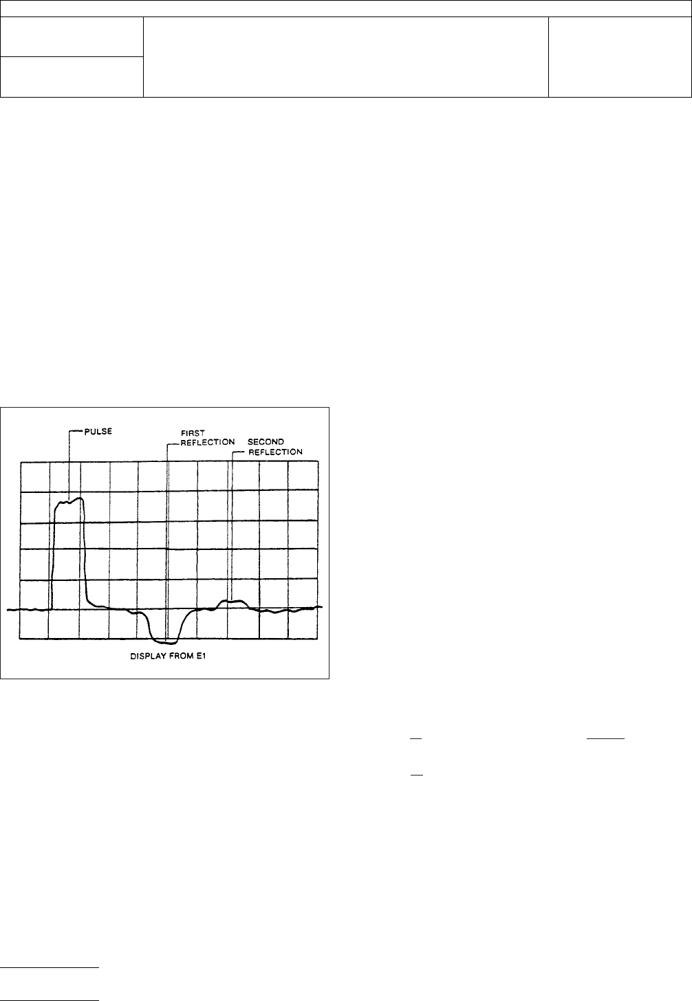
Apply
pulse specified and observe on the oscilloscope
connected to E
1
(see
Figure 4).
5.2.4
Set
the potentiometer R
2
for
minimum resistance,
observed on the scope at E
1
as
maximum mismatch (i.e.,
maximum negative first reflection).
5.2.5
Adjust
R
1
for
minimum second reflection.
5.2.6
Readjust
R
2
for
minimum first reflection.
5.2.7
Disconnect
the signal wires from the far end box
(receiver) and read and record the resistance values of R
1
and
R
2
.
5.2.8 Set
the potentiometers R
3
and
R
4
to
the value and
read at R
2
.
5.2.9
Reconnect
the sample to the receiver boxes and read
and record voltages at E
1
,E
2
,E
3
,
and E
4
.
Also read and
record the pulse rise time (10% to 90%) at E
1
and
E
2
.
5.3
Intralayer or Stacked Crosstalk
5.3.1
Place cables on Styrofoam base next to edge align-
ment block. The cables should be in close vertical alignment
(see Figure 3).
5.3.2 Place
the Styrofoam cover over the stack and with a
thin blade, push the cables against the edge piece all along
the length to assure the best possible vertical alignment. One
thousand gram weights are then placed at 0.3 m intervals on
top of the Styrofoam backing.
Note: The quality of the stack (vertical alignment and intimate
contact) should be checked before proceeding. This is done
by connecting a TDR to two grounds on the bottom layer and
the center signal wire on the top layer.
OSO
GOG
(Unused
wires are left open)
Any
indication of discontinuities on the scope indicates poor
alignment of the cables not in intimate contact.
5.3.3
Place
the box holding the bracket on the raisers so
that the height can be adjusted to provide a smooth transition
from the cables to the test fixtures.
5.3.4
Connect
the wires to the appropriate terminals on the
test fixtures and proceed as in 5.2.3.
Calculations:
CROSS TALK
Forward
E
4
E
1
(100)=%
Back
E
3
E
1
(100)=%
ATTENUATION
Voltage
E
4
− E
2
E
1
(100)=%
Rise
time E
2
(n.
sec.) - E
1
(n.
sec.) = n. sec.
Report:
Crosstalk is reported in percent fora3msample length.
Attenuation is reported in percent voltage and nanoseconds
rise time fora3msample length.
The report should also include the values of R
1
and
R
2
and
rise
time at E
1
.
IPC-2-5-21-3
Figure
4 Oscilloscope Display
IPC-TM-650
Number
2.5.21
Subject
Digital
Unbalanced Crosstalk, Flat Cable
Date
3/84
Revision
A
P
age2of2
电子技术应用 www.ChinaAET.com
1
Scope
This
test method is designed to determine the sur-
face insulation resistance of dielectric material after the pre-
scribed conditioning cycles.
2 Applicable Documents
MIL-STD-202
Method
106, Electronic Components
3
Test Specimens
3.1
At
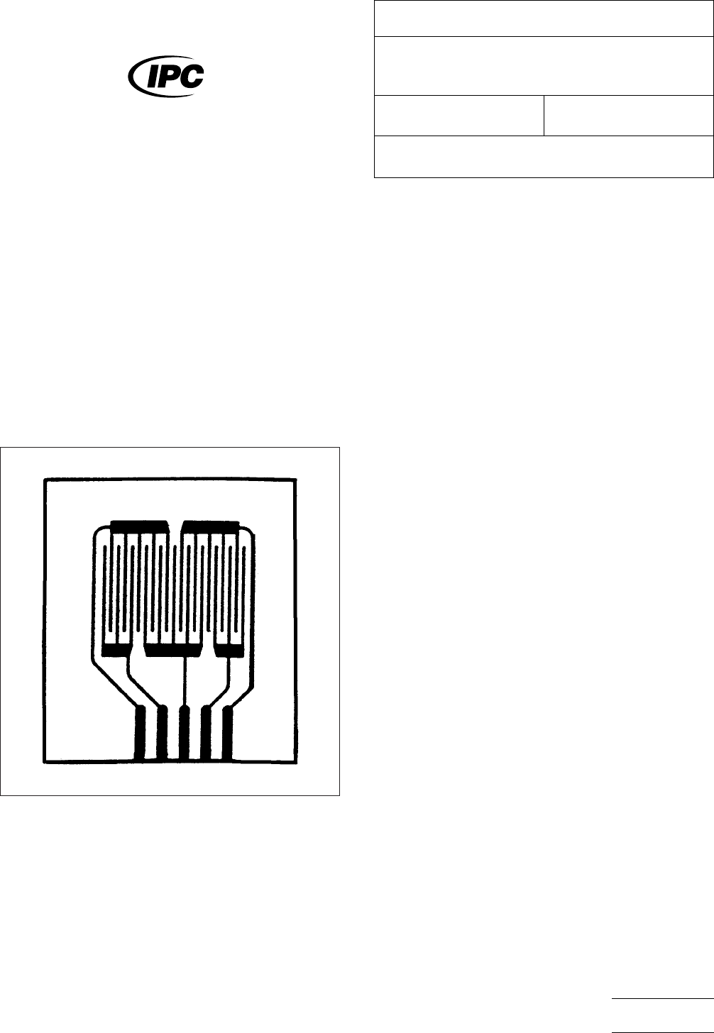
least two specimens, modeled after the IPC-B-25 (see
Figure 1) shall be made. The copper foil shall be removed by
chemical etching, using standard commercial practices.
4
Apparatus
4.1
A
test chamber capable of meeting MIL-STD-202,
Method 106, and elevated temperature of 150°C
4.2
A
meter capable of applying 500 VDC to the specimens
for a period of 60 +5/-0 seconds and measuring resistance
values between 1 megohm and 10 million megohms with
measurement error of less than 1% — A H/P Model 4329A,
High Resistance Meter, or equivalent
5 Procedure
5.1 Preparation
5.1.1
Double-clad
material shall have one side completely
etched. The other side and single-clad material shall be
etched as specified in 3.1.
5.1.2
Specimens
shall be dried for a period of 24 ± 2 hours
at 50°C ± 5°C. Measurements shall be made immediately
after removal from the chamber.
5.1.3
Specimens
shall be subjected to the conditioning
cycle of MIL-STD-202, Method 106 (except steps 7a and 7b).
The measurements shall be made inside the chamber after
completion of the cycle.
5.1.4 Specimens
shall be subjected to elevated temperature
for 24 hours at 150°C ± 5°C. Measurements shall be made
within 30 minutes after the completion of this cycle.
5.2
Test
5.2.1
Measurements
shall be made after each conditioning
phase. The specimens shall be removed from the chamber
before measurements specified in 5.1.2 and 5.1.4 are taken.
Specimens shall be left inside the chamber for taking mea-
surements specified in 5.1.3. Four readings per the comb pat-
tern shall be taken for each specimen; readings shall be
between pins1&2,1&3,3&5,and4&5(see Figure 1).
5.2.2
Turn
the megohmmeter on prior to the removal of the
specimens from the chamber. Allow the meter to warm up for
a minimum of 30 minutes.
5.2.3
After
warm-up, calibrate the meter and set the voltage
to 500 VDC.
5.2.4
Connect
the leads to the appropriate pins (see Figure
1).
IPC-2-5-27-1
Figure
1 Surface Insulation Resistance Test Pattern
(Modeled
after IPC-B25 Test Board)
The
Institute for Interconnecting and Packaging Electronic Circuits
2215 Sanders Road • Northbrook, IL 60062
IPC-TM-650
TEST
METHODS MANUAL
Number
2.5.27
Subject
Surface
Insulation Resistance of Raw Printed
Wiring Board Material
Date
3/79
Revision
Originating Task Group
Material
in this Test Methods Manual was voluntarily established by Technical Committees of the IPC. This material is advisory only
and its use or adaptation is entirely voluntary. IPC disclaims all liability of any kind as to the use, application, or adaptation of this
material. Users are also wholly responsible for protecting themselves against all claims or liabilities for patent infringement.
Equipment referenced is for the convenience of the user and does not imply endorsement by the IPC.
P
age1of2
电子技术应用 www.ChinaAET.com