IPC-TM-650 EN 2022 试验方法.pdf - 第560页
Number Subject Date Revision Originating T ask Group Material in this T est Methods Manual was voluntarily established by T echnical Committees of IPC. This material is advisory only and its use or adaptation is entirely…

9) Conduct the short trace characterization from Step 4.
10) Post-process the results using methods described in
Section 1.2.2.
Note: The humidity is controlled at RH of 50% (±5%) for all
data points, except for 0 and 100 °C.
5.7 Test Report Below is an example of the list of informa-
tion to be included in the test report. The actual format and
information to be included in the test report may vary based
on the requirement of specific customer:
• VNA Settings: test frequency range, step size, IF bandwidth,
etc.
• Probing method: handheld probe, microwave probe, or
printed board mounted co-axial connector without probes
• Manufacturer and part number of the probe (if used), and
the bandwidth of the probe per 4.2
• Condition of test samples per 3.8.1 or 3.8.2
• Temperature and humidity of testing condition for Room-
Temperature test
• Temperature and humidity of testing condition for Varying-
Temperature test per 5.6
• Calibration or de-embedding method per 1.2.2 or 1.3.1 or
1.3.2
• Insertion loss fitting method per 5.4.2 or 5.4.3
• Values of the insertion loss at test frequencies, in dB/inch or
dB/cm
• Uncertainty estimate at test frequencies per 5.4.4
• Any anomalies in the test or variations from this test method
6 Reference Documents
[1] N. R. Franzen, R. A. Speciale, ‘‘A New Procedure for
System Calibration and Error Removal in Automated
S-Parameter Measurements,’’ Proceedings of the 5th
European Microwave Conference, Hamburg, Germany,
1-4 September 1975, pp. 69-73.
[2] R. A. Soares, P. Gouzien, P. Legaud, G. Follot ‘‘A Unified
mathematical approach to two-port calibration tech-
niques and some applications,’’ IEEE Trans. on MTT, v.
37, N 11 1989, pp. 1669-1674.
[3] R. B. Marks, ‘‘A Multiline Method of Network Analyzer
Calibration,‘‘ IEEE Transactions on Microwave Theory
and Techniques 39, pp. 1205-1215, July 1991.
[4] C. Seguinot et al.: – Multimode TRL ‘‘A new concept in
microwave measurements’’
[5] D. Degroot, J. Jargon, R. Marks, ‘‘Multiline TRL
revealed,’’ 60th ARFTG Conference Digest, Fall 2002.
[6] Y. Shlepnev, ‘‘Broadband material model identification
with GMS-parameters’’, 2015 IEEE 24th Conference on
Electrical Performance of Electronic Packaging and Sys-
tems (EPEPS’2015), October 25-28, 2015, San Jose,
CA.
[7] G. F. Engen and C. A. Hoer, ‘‘Thru-Reflect-Line: An
Improved Technique for Calibrating the Dual Six-Port
Automatic Network Analyzer,‘‘ Microwave Theory and
Techniques, IEEE Transactions on, vol. 27, pp.987-993,
1979.
[8] V. Adamian, B. Cole, ‘‘A Novel Procedure for Character-
ization of Multiport High Speed Balanced Devices,’’
DesignCon, San Jose, CA, 2007.
[9] H. Barnes, E. Bogatin, J. Moreira, J. Ellison, et al. ‘‘A
NIST Traceable PCB Kit for Evaluating the Accuracy of
DeEmbedding Algorithms and Corresponding Metrics,’’
DesignCon 2018.
[10] X. Ye, J. Fan and J. Drewniak, ‘‘New De-embedding
Techniques for PCB Transmission-Line Characteriza-
tion’’, DesignCon 2015.
[11] IEEE P370 open-source 2X-Thru de-embedding code,
https://gitlab.com/IEEE-SA/ElecChar/P370.
[12] https://standards.ieee.org/standard/370-2020.html
[13] S. Moon, X. Ye, R. Smith, ‘‘Comparison of TRL Calibra-
tion vs. 2X-Thru De-embedding Methods,’’ IEEE Interna-
tional Symposium on EMC and SI, 2015.
[14] A. Koul, M. Koledintseva, S. Hinaga, J. Drewniak, ‘‘Dif-
ferential Extrapolation Method for Separating Dielectric
and Rough Conductor Losses in Printed Circuit
Boards,’’ IEEE Transaction on Electromagnetic Compat-
ibility, Vol. 54, No. 2, April 2012.
[15] X. Ye, M. Balogh, ‘‘Physics-Based Fitting to Improve
PCB Loss Measurement Accuracy,’’ IEEE International
Symposium on EMC, 2017.
IPC-TM-650
Number
2.5.5.14
Subject
Measuring High Frequency Signal Loss and Propagation on
Printed Boards with Frequency Domain Methods
Date
02/2021
Revision
Page 11 of 11
Number
Subject
Date Revision
Originating Task Group
Material in this Test Methods Manual was voluntarily established by Technical Committees of IPC. This material is advisory only
and its use or adaptation is entirely voluntary. IPC disclaims all liability of any kind as to the use, application, or adaptation of this
material. Users are also wholly responsible for protecting themselves against all claims or liabilities for patient infringement.
Equipment referenced is for the convenience of the user and does not imply endorsement by IPC.
3000 Lakeside Drive, Suite 105 N
Bannockburn, Illinois 60015-1249
IPC-TM-650
TEST METHODS MANUAL
1 Scope
This test method describes a way to measure the relative permittivity (
e
r
) and loss tangent (tan
d
) (also called dielectric constant,
Dk, and dissipation factor, Df) of base materials for printed boards at frequencies from 1 GHz to 20 GHz using a split post
dielectric resonator (SPDR).
2 Applicable Documents
2.1 IPC-TM-650 Method 2.5.5.2 Dielectric Constant and Dissipation Factor of Printed Wiring Board Material –
Clip Method
2.2 IPC-TM-650 Method 2.5.5.3 Permittivity (Dielectric Constant) and Loss Tangent (Dissipation Factor) of Materials
(Two Fluid Cell Method)
2.3 IPC-TM-650 Method 2.5.5.5 Stripline Test for Permittivity and Loss Tangent (Dielectric Constant and Dissipation Factor)
at X-Band
2.4 IPC-TM-650 Method 2.5.5.5.1 Stripline Test for Complex Relative Permittivity of Circuit Board Materials to 14 GHz
2.5 IPC-TM-650 Method 2.5.5.9 Permittivity and Loss Tangent, Parallel Plate, 1MHz to 1.5 GHz
3 Test Specimens
3.1 All base materials specimens shall have the metallic foil layer removed by etching or other suitable means and shall be
thoroughly cleaned. Each specimen shall be marked in the upper left corner with an engraving pencil or equivalent.
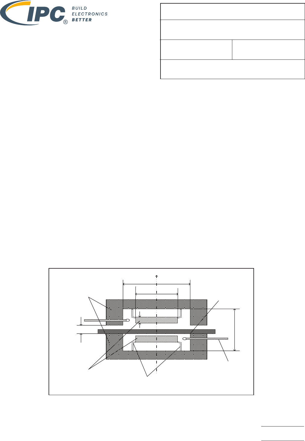
3.2 The dimensions of the test specimen shall be larger than the outer dimension of the fixture. See Figure 1.
The size of the specimen shall be larger than the internal diameter D of the metal enclosures, and the maximum thickness of the
specimen shall be smaller than the distance h
g
between the metal enclosures of the fixture.
support
coupling loop
metal enclosure
dielectric resonators
sample
D
h
g
z
h
r
L
dr
Figure 1 – Diagram of SPDR Test Fixture
Page 1 of 7
2.5.5.15
06/22 N/A
3-11a IPC-4101 Task Group
Relative Permittivity and Loss Tangent Using a
Split-Post Dielectric Resonator
IPC-TM-650
Number Subject Date
Revision
where
h
g
is the distance between the metal enclosures of the fixture;
D is internal diameter of the metal enclosures;
L is internal height of the metal enclosures;
d
r
is the diameter of the dielectric resonator;
h
r
is the thickness of the dielectric resonator.
3.3 Specimen Thickness The thicker the specimen the less error occurs in the measurements. A thin specimen may be stacked
up to a minimum of 0.4 mm [0.016 in] to improve measurement accuracy. The air gaps between the sample and the fixture do
not affect the measurement.
3.4 Number of Specimens Three specimens for the test at room temperature and one specimen for the test at variable temperatures
are required for each SPDR test fixture for this test. Table 1 shows the supported specimen dimensions
Table 1 – Specimen Dimensions
Nominal Frequency [GHz]
Specimen Sizes
mm [inch]
Maximum Thickness
mm [inch]
1 150 X 150 [5.9 X 5.9] 6.0 [0.24]
3 80 X 80 [3.2 X 3.2] 3.0 [0.12]
5 to 6 80 X 80 [3.2 X 3.2] 2.0 [0.08]
9 to 10 80 X 80 [3.2 X 3.2]
0.9 [0.035]
13 to 16 50 X 35 [2.0 X 1.4] 0.6 [0.024]
18 to 20 15 X 15 [0.6 X 0.6] 0.5 [0.020]
2.5.5.15 Relative Permittivity and Loss Tangent Using a 06/22
Split-Post Dielectric Resonator
N/A
Page 2 of 7