IPC-TM-650 EN 2022 试验方法.pdf - 第642页
1 Scope The Power Density Rating (PDR) for Embedded Resistors test method covers procedures for the demonstra- tion of the ability to operate the embedded device safely, with- out a permanent change in the electrical cha…
IPC-2.5.33.4-3
Figure
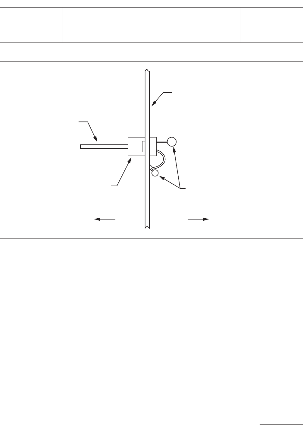
3 Test Electrode Mounting Suggestion
MET
AL
ENCLOSURE WALL
WIRE LOOPS
TO CONNECT SCOPE
PROBE AND GROUND CLIPS
OutsideInside
TEST
ELECTRODE
BOARD
DUAL READOUT
PANEL MOUNT
EDGE CARD CONNECTOR
IPC-TM-650
Number
2.5.33.4
Subject
Measurement
of Electrical Overstress from Soldering Hand
Tools - Shielded Enclosure
Date
11/98
Revision
P
age3of3
电子技术应用 www.ChinaAET.com

1 Scope The Power Density Rating (PDR) for Embedded
Resistors test method covers procedures for the demonstra-
tion of the ability to operate the embedded device safely, with-
out a permanent change in the electrical characteristic of the
device. The procedure consists of monitoring a resistance
change from its nominal value as a function of the dissipated
power. During the test, the applied voltage or current stimulus
is held until the device temperature is stable, the steady resis-
tance reading is reached, and the dissipated power is mea-
sured. This process is repeated with higher dissipated power
until the measured resistance change exceeds the specifica-
tion limits. The results are presented in terms of the dissipated
power density rating (PDR) factor for the embedded resistive
device.
This document describes testing procedure for power density
rating of embedded resistive devices, which operate in com-
plex electrical and thermal environments, and for which exist-
ing procedures are not adequate or inapplicable.
2 Applicable Documents
IPC-4811
Specification for Embedded Passive Device Resis-
tor Materials for Rigid and Multilayer Printed Boards
IPC-TM-650 Test Methods Manual
1.3 Ambient Conditions
3 Terminology When current passes through a resistor,
electrical energy is dissipated by the resistor in the form of
heat. A resistor can be used at any combination of voltage
and current as long as its dissipating power (P) does not
exceed the maximum power rating (P
max
) indicating how
much power the resistor can convert into heat and absorb
or/and transfer away without any damage to itself or to the
surrounding circuitry.
3.1 Electrical Resistance, R
R = V / I (1)
R is a ratio of voltage V over current I, (Ohm’s law), the unit of
measure is ohm [Ω].
3.2 Dissipated Power, P
Direct current (DC):
P = VI; P = V
2
/ R; P = I
2
R (2)
Alternating current (AC):
P = V* I* cos (ϕ) (3)
V* and I* are voltage and current amplitudes, and ϕ is the
phase angle between V* and I*.
3.3 Power Density Rating The power density rating (PDR)
is defined as the total dissipated power normalized by the
effective surface area (heat flux cross sectional area).
PDR = P
max
/ S (4)
where, S is the area of the embedded resistor or device
defined as one-side of the heat flux area.
3.4 Power Density Rating Comments
• The power that can be dissipated by a resistor is limited by
the size of the resistor and the maximum operational tem-
perature of the resistive material.
• The power ratings depend on thermal management of the
heat generated from the resistor.
• The use of heat sinks can lower the device’s operating tem-
perature and consequently increase the power rating.
• Higher glass transition temperature laminate materials in
which the resistive device is embedded can allow higher
operating temperatures.
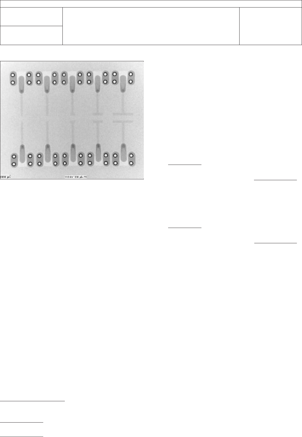
4 Test Specimen This method recommends testing the
embedded resistors in configurations that reflect the actual
functional application (Figure 1).
The recommended geometrical attributes of the embedded
resistors are specified in the IPC-4811.
4.1 Sampling The sampling procedure for the tested
specimen should be defined in the specification for that
device. The sampling procedure should provide sufficient data
to estimate the average quality and the variability of the lot
being examined.
4.2 Conditioning The test results can be influenced by
temperature, moisture content and other electrically active
residuals originating from the processing conditions such as
3000 Lakeside Drive, Suite 309S
Bannockburn, IL 60015-1249
IPC-TM-650
TEST METHODS MANUAL
Number
2.5.34
Subject
Power Density Rating for Embedded Resistors
Date
07/12
Revision
Originating Task Group
Embedded Devices Test Methods Subcommittee
(D-54)
Material in this Test Methods Manual was voluntarily established by Technical Committees of IPC. This material is advisory only
and its use or adaptation is entirely voluntary. IPC disclaims all liability of any kind as to the use, application, or adaptation of this
material. Users are also wholly responsible for protecting themselves against all claims or liabilities for patent infringement.
Equipment referenced is for the convenience of the user and does not imply endorsement by IPC.
Page1of4
plating, circuit developing baths and soldering re-flows. Mate-
rials so affected should be brought to equilibrium with appro-
priate atmosphere and temperature control before testing.
Description of the conditioning should be included in the test-
ing report.
5 Apparatus The method requires a power source meter
and electrical resistance meter, such as Keithley
1
Source
Meter or equivalent, for sourcing the applied DC power and
measuring the resulting current resistance. The resolution
of resistance measurements should be in the range of about
0.1 Ω or better.
5.1 Power requirements The power capacity of the
power sourcing instrumentation should be sufficient to main-
tain the test power until it reaches the value defined in the test
failure/acceptance criteria where the specimen-maximum
power will be dissipated. The voltage level should be stable to
within ± 0.1% of the set value during the testing time. An out-
put current of 1 µA to1Aisusually sufficient for most testing
conditions. The power dissipated during the test may vary
depending on the specimen resistance thermal characteris-
tics, and the failure mechanism.
5.2 Circuit controls The apparatus should be equipped
with a circuit breaking device with adjustable current/voltage
sensors, and be capable of disconnecting the power source
in the case of overloading conditions. The current/voltage-
sensing circuit should measure the specimen power and allow
for adjustment consistent with the specimen characteristics.
The sensing device should respond at the power level that is
indicative of the test conditions reaching the failure criteria.
5.3 Power level controls The power level should be
adjustable with the possibility of setting discrete power level
values in at least 20 steps. It is recommended that the initial
power P
0
is set at 1/10 of the nominal operational power of
the device. A computerized experimental set-up is recom-
mended to carry out the test.
In the case of sourcing voltage, the initial voltage, V
0
=
√
0.1
*
P
nom
*
R
0
. For example, if the initial value of R
0
=50
Ω and P
nom
= 0.1 W then the initial voltage V
0
corresponding
to 0.1 of P
nom
(i.e., P
0
= 0.010 W), is
√
0.1
*
0.1 W
*
50 Ω≈
0.7 V. The voltage level V
n
should be increased in steps of V
s
≤ V
0
, each step having duration of about 60 s. The specimen
current I
n
should be monitored and recorded at every power
step (see 5.3.1).
In the case of sourcing current, the initial current, I
0
=
√
0.1
*
P
nom
/ R
0
. For example, if the initial value of R
0
=50
Ω and P
nom
= 0.1 W, then the initial voltage V
0
corresponding
to 0.1 of P
nom
(i.e., P
0
= 0.010 W), is
√
0.1
*
0.1 W / 50 Ω≈
0.014 A. The current level I
n
should be increased in steps of I
s
≤ I
0
, each step having a duration of about 60 s. The specimen
voltage V
n
should be monitored and recorded at every power
step (see 5.3.2).
5.3.1 Linear Voltage Steps Increasing voltage in constant
voltage steps will result in a quadratic increase of power. At
the n
th
voltage step the power P
n
is given by (5):
P
n
=(V
0
+ nV
s
)
2
/ R
n
(5)
Example: R
n
= R
0
=50Ω, V
0
= 0.7 V, V
s
= 0.3 V. At n =11
step V
11
= 4 V and the corresponding applied power P
11
=
(0.7V+11
*
0.3V)
2
/50Ω = 0.32 W.
5.3.2 Linear Current Steps Increasing current from I
0
by
adding a constant current step, I
s
, will result in a quadratic
increase of applied power. At the n
th
current step the power
P
n
is given by (6):
P
n
=(I
0
+ nI
s
)
2
*
R
n
(6)
1. Certain commercial equipment and materials are identified in this document in order to specify adequately the experimental procedure. In no case does such
identification imply recommendations nor does it imply that the material or equipment identified is necessarily the best available for this purpose.
Figure 1 An X-Ray Image of Thin Film Resistors
Embedded Inside a Printed Circuit Board
IPC-TM-650
Number
2.5.34
Subject
Power Density Rating for Embedded Resistors
Date
07/12
Revision
Page2of4