IPC-TM-650 EN 2022 试验方法.pdf - 第305页
5.3 Calculation of Results 5.3.1 Average Bow and Twist Results Bow and Twist = Sum of the Measured Maximum Vertical Displacements in mm [in] Number of Test Specimens 5.3.2 Maximum Bow and Twist Results The maximum vertic…
1.0
Scope
This
method covers the measurement of bow
and twist by maximum vertical displacement of an unre-
strained panel of either cut to size panels or finished rigid
printed boards including single- and double-sided, multilayer,
and the rigid segments of rigid flex printed circuits. This test
method is only applicable to laminates greater than or equal to
0.5 mm [0.020 in] in thickness. This test method can also be
used after etching or after thermal stress with requirements as
agreed between user and vendor.
2.0
Applicable Documents
None
3.0 Test Specimen
The
test specimen for incoming
inspection shall be 300 x 300 mm ± 2mm[12x12in±0.08
in] in size. For smaller panel sizes and finished printed wiring
boards, use actual size. A minimum of three specimens is
required per sample, when evaluating pressed laminate
sheets.
4.0
Apparatus
4.1
Sample
Shear
4.2
Granite
Surface Plate or Equivalent
4.3
Feeler
Gauges or Equivalent
4.4
Micrometer
5.0
Test Procedure
5.1 Preparation of the Test Specimen
5.1.1
For
laminate sheet, the test specimens are to be cut
in such a fashion as to minimize mechanical flexing.
5.1.2
For
cut to size panels or printed wiring boards, use
actual size.
5.1.3
Mark
the specimen for traceability. No mechanical or
chemical pre-cleaning is permitted on the specimens.
5.2
Measurement of Bow and Twist
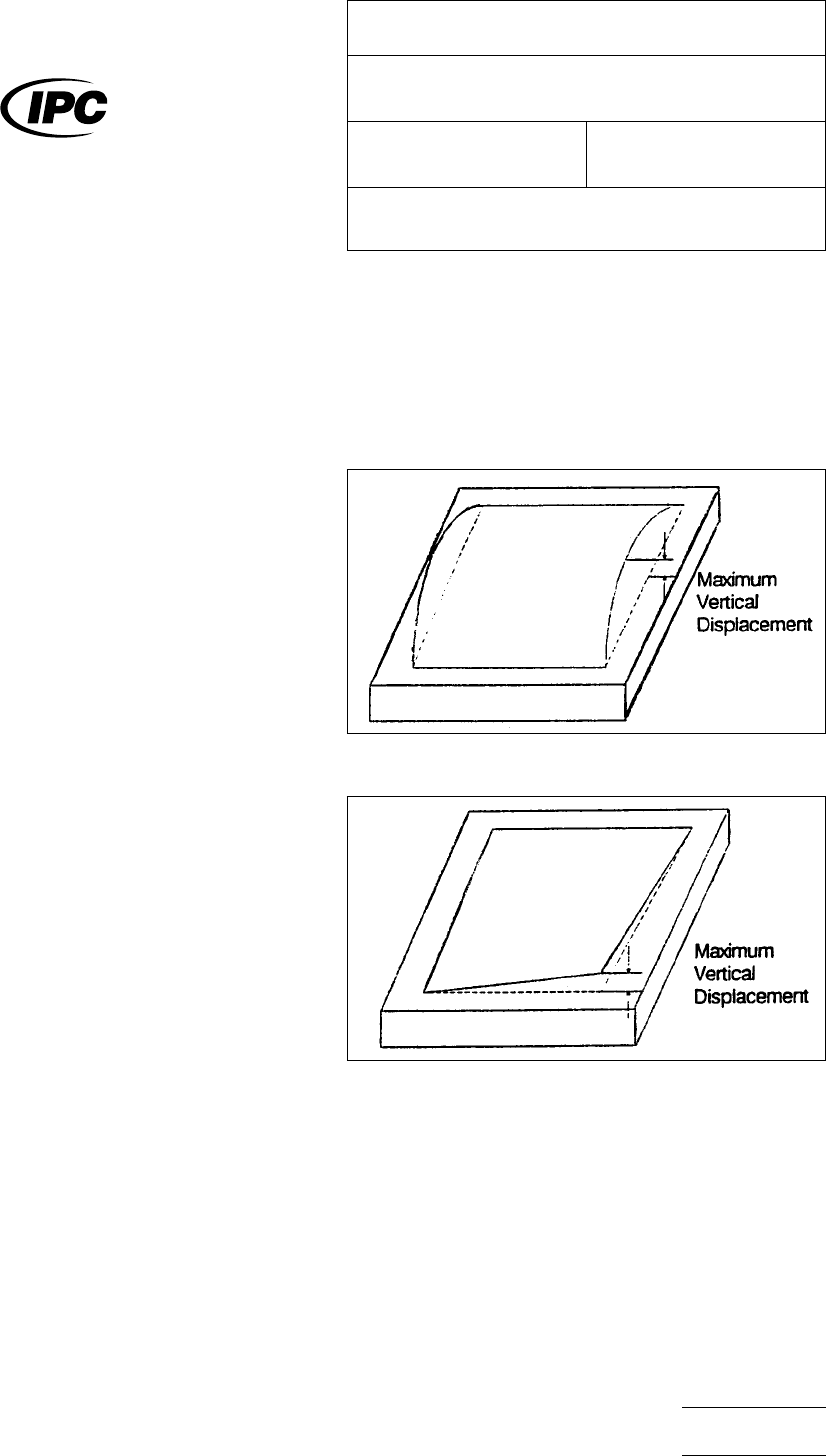
5.2.1
Place
the test panels on the surface plate such that
the maximum vertical displacement is observed. The panel
should be turned over in establishing the maximum vertical
displacement. The maximum vertical displacement may be a
corner or a side of the test specimen as illustrated in Figures
1 and 2.
5.2.2
Measure
the maximum vertical displacement by
inserting the feeler gauges between the surface plate and the
bottom surface of the laminate.
5.2.3
Verify
the thickness measurement by measuring the
total thickness of the feeler gauges with the micrometer.
5.2.4
Record
the maximum vertical displacement in 0.25
mm [0.01 in]. One value is recorded per test specimen. This is
the bow and twist of the test specimen.
IPC-24221-1
Figure
1
IPC-24221-2
Figure
2
The
Institute for Interconnecting and Packaging Electronic Circuits
2215 Sanders Road • Northbrook, IL 60062-6135
IPC-TM-650
TEST
METHODS MANUAL
Number
2.4.22.1
Subject
Bow
and Twist—Laminate
Date
5/93
Revision
C
Originating Task Group
Material
in this Test Methods Manual was voluntarily established by Technical Committees of the IPC. This material is advisory only
and its use or adaptation is entirely voluntary. IPC disclaims all liability of any kind as to the use, application, or adaptation of this
material. Users are also wholly responsible for protecting themselves against all claims or liabilities for patent infringement.
Equipment referenced is for the convenience of the user and does not imply endorsement by the IPC.
P
age1of2
电子技术应用 www.ChinaAET.com

5.3
Calculation of Results
5.3.1 Average Bow and Twist Results
Bow and Twist =
Sum of the Measured Maximum
Vertical Displacements in mm [in]
Number
of Test Specimens
5.3.2
Maximum Bow and Twist Results
The
maximum
vertical displacement in mm [in] obtained for each lot of
material.
6.0 Notes
6.1
This
is the referee method; other methods of measure-
ment are allowable, if agreed upon between user and vendor.
IPC-TM-650
Number
2.4.22.1
Subject
Bow
and Twist—Laminate
Date
5/93
Revision
C
P
age2of2
电子技术应用 www.ChinaAET.com

1.0
Scope
This
test method establishes a procedure for
determining the flatness of silicon wafers coated with depos-
ited organic films.
2.0
Applicable Documents
ASTM D 618
Standard
Practice for Conditioning Plastics and
Electrical Insulating Materials for Testing
3.0
Test Specimen
The
test specimens are 125 mm diam-
eter silicon wafers 625 ± 15 µm in thickness. The surface of
the wafers must be clean, and at least one side of the wafers
must be polished. A minimum of 9 wafers are required.
4.0
Apparatus or Material
4.1 Radius Of Curvature Measurement Device
Flexus
Thin
Film Stress Measuring Apparatus (TFSMA) Model 2-300
or equivalent.
4.2
Wafer Thickness Measurement Device
Micrometer
capable
of measuring accurately to 5 µm. A thickness gauge
including weights can also be purchased from Flexus that can
be used with the TFSMA to measure thickness.
4.3
Film Thickness Measurement Device
Nanospec
Model
210, Tencor AlphaStep, or equivalent film thickness
measurement device capable of measuring accurately to 0.1
µm.
5.0
Procedure
5.1 Radius Of Curvature Of Uncoated Wafers
5.1.1
Label
each wafer with a unique identification.
5.1.2
Measure
the thickness of the uncoated silicon wafers.
5.1.3
Measure
the radius of curvature of the uncoated
wafers following the manufacturers recommended procedure.
5.2
Coat Wafers
5.2.1
Use
a minimum of three film thicknesses for each
polymer or processing condition investigated. The film thick-
nesses should span as large a range as possible, e.g., 5, 10
and 15 µm. Coat at least three wafers for each film thickness
for a minimum of nine wafers.
5.2.2 Coat
the polymer solution onto the back (unpolished
side) of the silicon wafers using manufacturer s recommended
deposition technique (e.g., spin coating). Process the coating
according to the manufacturer s recommended procedures.
The final film thickness must not vary by more than 2% across
the substrate surface.
5.3
Radius of Curvature Of Coated Wafers
5.3.1
The
coated wafers should be conditioned at 23 ± 2°C
and 50 ± 5% relative humidity for exactly 24 hours prior to
testing. Many polymers exhibit stress relaxation or a decrease
in stress associated with moisture absorption, therefore it is
essential that the coated wafers are equilibrated under identi-
cal conditions. Refer to ASTM D 618.
5.3.2
Measure
the radius of curvature of the coated wafers
following the equipment manufacturer’s recommended proce-
dure. Correct placement of the wafers in the device is essen-
tial to compensate for nonuniform wafers, therefore the wafer
must be placed in the same position for each measurement.
At this point the coating thickness is unknown; however,
some value may be required by the curvature measurement
device. Use whatever number is convenient for now, the data
will be edited later.
5.3.3
Repeat
step 5.3.1 four (4) times for each wafer. The
reason for the repeated measurements is to generate an aver-
age to compensate for errors in placing the wafer in the cur-
vature measurement device at the exact position in which it
was originally measured during step 5.1.3.
5.4
Film Thickness Measurements
Measure
the film
thickness on each coated wafer to an accuracy of 0.1 µmor
better using the film thickness measurement device. The
thickness should be measured at several different locations to
compensate for nonuniform coatings.
5.7
Calculations
The
Institute for Interconnecting and Packaging Electronic Circuits
2215 Sanders Road • Northbrook, IL 60062-6135
IPC-TM-650
TEST
METHODS MANUAL
Number
2.4.22.2
Subject
Substrate
Curvature: Silicon Wafers with Deposited
Dielectrics
Date
7/95
Revision
Originating Task Group
Deposited Dielectric Task Group (C-13a)
Material
in this Test Methods Manual was voluntarily established by Technical Committees of the IPC. This material is advisory only
and its use or adaptation is entirely voluntary. IPC disclaims all liability of any kind as to the use, application, or adaptation of this
material. Users are also wholly responsible for protecting themselves against all claims or liabilities for patent infringement.
Equipment referenced is for the convenience of the user and does not imply endorsement by the IPC.
P
age1of2
电子技术应用 www.ChinaAET.com