IPC-TM-650 EN 2022 试验方法.pdf - 第668页
In addition, there shall be at least two unprocessed control coupons for comparison purposes (Table 1, Sample Group F). 5.2.1 Positive, permanent and noncontaminating identifica- tion of test specimens is of paramount im…
1
Scope
This
test method is to characterize fluxes by
determining the degradation of electrical insulation resistance
of rigid printed wiring board specimens after exposure to the
specified flux. This test is carried out at high humidity and heat
conditions.
2
Applicable Documents
IPC-B-24
Surface
Insulation Resistance Test Board
IPC-A-600
Acceptability
of Printed Boards
IPC
J-STD-004
Requirements
for Soldering Fluxes
IPC-9201
Surface
Insulation Resistance Handbook
3
Test Specimen
A
minimum of 10 ml of liquid flux, a rep-
resentative container of solder paste, cored wire, paste flux, or
extracted solder preform flux. The reflow/extraction process
should be carried out in accordance with IPC J-STD-004.
3.1
Comb Patterns
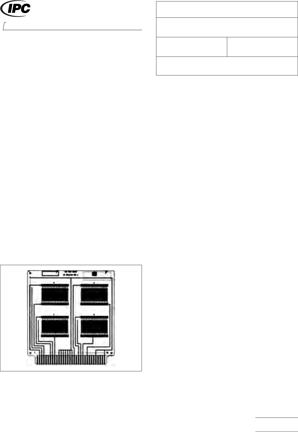
Use
the IPC-B-24 test pattern (see
Figure 1), which consists of four comb patterns per coupon.
Each individual comb has 0.4 mm lines and 0.5 mm spacing.
The metallization shall be unpreserved bare copper.
3.2
Laminat
The
laminate material for this test shall be
FR-4 epoxy-glass.
4
Apparatus
4.1
A
clean test chamber capable of programming and
recording an environment of 25 +10/-2 °C [77 + 18/-3 °F] to
at least 85 ± 2 °C [185 ± 3.6 °F] and 20% ± 5% to 85% ± 2%
relative humidity. A salt solution and desiccator may be used
to maintain humidity if a tight temperature control is main-
tained on the chamber.
4.2
A
power supply capable of producing a standing bias
potential of 45-50 volts DC with a tolerance of ± 10%.
4.3
A
resistance meter capable of reading high resistance
(10
12
ohms)
with a test voltage of 100 volts, or an ammeter
capable of reading 10
-10
amps
in combination with 100 volts
DC power supply.
4.4
Three
2000 ml beakers.
4.5
Exhaust
ventilation hood.
4.6
Metal
tongs.
4.7 Soft
bristle brush.
4.8
Deionized
or distilled water (2 megohm-cm minimum
resistivity recommended).
4.9
Drying
oven capable of maintaining at least 50 °C
[122 °F].
5
Procedure
5.1 Test Conditions
All
fluxes will be tested at 85 ± 2 °C,
[185 ± 3.6 °F], 85 ± 2% relative humidity for 168 hours.
5.2
Specimen Preparation
There
shall be three test cou-
pons for each liquid flux to be tested in the cleaned state
(Table 1, Sample Group A). When testing liquid fluxes which
are intended to remain in the uncleaned state, six test cou-
pons are required. Three uncleaned test coupons shall be
soldered pattern side down (Table 1, Sample Group B) and
three shall be soldered pattern side up (Table 1, Sample
Group C).
Solder paste coupons shall be reflowed pattern side up and
either cleaned (Table 1, Sample Group D) or not cleaned
(Table 1, Sample Group E).
IPC-2633-1
Figure
1 Test Pattern from IPC-B-24
2215
Sanders Road
Northbrook, IL 60062-6135
IPC-TM-650
TEST
METHODS MANUAL
Number
2.6.3.3
Subject
Surface
Insulation Resistance, Fluxes
Date
06/04
Revision
B
Originating Task Group
Flux Specifications Task Group, (5-24a)
Material
in this Test Methods Manual was voluntarily established by Technical Committees of IPC. This material is advisory only
and its use or adaptation is entirely voluntary. IPC disclaims all liability of any kind as to the use, application, or adaptation of this
material. Users are also wholly responsible for protecting themselves against all claims or liabilities for patent infringement.
Equipment referenced is for the convenience of the user and does not imply endorsement by IPC.
P
age1of4
ASSOCIA
TION CONNECTING
ELECTRONICS INDUSTRIES
®
电子技术应用 www.ChinaAET.com
In
addition, there shall be at least two unprocessed control
coupons for comparison purposes (Table 1, Sample Group F).
5.2.1
Positive,
permanent and noncontaminating identifica-
tion of test specimens is of paramount importance. (For
example, a vibrating scribe.) Permanent ink may be used on
the back side of the test coupon if areas beneath conductors
are avoided.
5.2.2
Visually
inspect the test specimens for any obvious
defects, as described in IPC-A-600. If there is any doubt
about the overall quality of any test specimen, the test speci-
men should be discarded.
5.2.3
Clean
each test or control coupon with deionized or
distilled water and scrub with a soft bristle brush for a mini-
mum of 30 seconds. Spray rinse thoroughly with deionized or
distilled water. Rinse the cleaned area thoroughly with fresh
2-propanol.
An alternative cleaning method is to place the test coupon in
an ionic contamination tester containing 75% 2-propanol,
25% deionized water and process the solution until all ionics
have been removed.
During the remainder of the specimen preparation, handle test
specimens by the edges only, and use noncontaminating rub-
ber gloves.
5.2.4
Dry
the cleaned boards for two hours at 50 °C
[122 °F].
5.2.5 If
boards are to be stored before treatment, place the
boards in Kapak® bags or other contamination-free contain-
ers (do not heat seal) in a desiccator.
5.3
Sample Preparation
Flux
application and soldering.
5.3.1
Liquid Flux or Flux Extract
Coat
the test pattern
with a thin coating of the liquid flux or flux extract under test.
5.3.1.1
Preheat
the flux coated test coupon using the tem-
perature profile recommended by the vendor. If no profile is
available, preheat the test coupon in an oven set at a tem-
perature such that the test coupon reaches a temperature of
140 °C [284 °F] in 30 to 45 seconds.
5.3.1.2 Immediately
expose the test coupon to solder by
floating the fluxed comb patterns of the test specimen face
down on the solder pot at 245-260 °C [473-500 °F] for4±1
seconds. Be sure that all dross is removed from the solder pot
surface just before contact with the specimen.
5.3.1.3
Alternatively,
the specimen can be wave soldered
face down at 245-260 °C [473-500 °F] and a conveyor speed
with a contact time of3±1seconds.
5.3.1.4
For
fluxes to be tested in the uncleaned state, a
second set of test patterns shall be fluxed and floated pattern
up on the solder pot or passed pattern up over the solder
wave.
5.3.2 Solder Paste or Paste Flux
Stencil
print the solder
paste or paste flux onto the comb pattern using a 0.15 mm
[0.00591 in] (6 mil) thick stencil (the IPC-A-24 artwork con-
tains the stencil design).
5.3.2.1
The
samples shall be run through a reflow soldering
process using the temperature profile recommended by the
vendor.
5.3.3
Cored Wire
Using
a clean fine-tip soldering iron
apply the cored wire to the comb patterns being careful not to
bridge the conductors. The iron temperature should be as
specified by the cored wire vendor.
5.4
Cleaning of Samples
5.4.1
After
exposure to flux and solder, samples to be
tested in an uncleaned state shall be tested as outlined in 5.5
through 5.6.1.
5.4.2
After
exposure to flux and solder, samples to be
tested in the cleaned state shall be cleaned using one of the
T
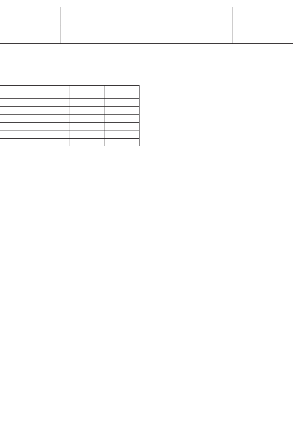
able 1 Coupons for SIR Testing
Sample
Group
Flux/
Solder
Clean
Number of
Coupons
A
Yes Yes 3
B Yes No 3
C Yes No 3
D Yes Yes 3
E Yes No 3
FNoNo2
A
= Pattern down/cleaned
B = Pattern down/not cleaned
C = Pattern up/not cleaned
D = Solder paste/reflow/cleaned
E = Solder paste/reflow/not cleaned
F = Control (precleaned, unprocessed)
IPC-TM-650
Number
2.6.3.3
Subject
Surface
Insulation Resistance, Fluxes
Date
06/04
Revision
B
P
age2of4
电子技术应用 www.ChinaAET.com

procedures
listed below. The cleaning parameters shall be
reported in the Qualification Test Report of J-STD-004.
5.4.2.1
The
samples to be cleaned shall be cleaned with an
appropriate environmentally safe solvent or aqueous cleaning
medium. The use of a commercial in-line or batch cleaner is
preferred. If this is not available, the following laboratory clean-
ing process shall be followed.
5.4.2.2
Samples
shall be cleaned within 30 minutes or less
after soldering. For solvent or aqueous detergent cleaning,
three 2000 ml beakers each containing 1000 ml of solvent
shall be used such that one beaker serves as the primary
cleaning stage and the other two are used for rinsing pur-
poses. Each test coupon shall be agitated in each beaker for
one minute. In the case of aqueous detergent, one beaker
shall contain the cleaning agent and the remaining beakers
shall contain deionized water for rinsing purposes. Beaker
solutions shall be used to clean or rinse a maximum of three
specimens before the solutions are replaced. After the clean-
ing procedure, dry the samples for two hours at 50 °C
[122 °F]. Following cleaning and drying, the specimens shall
be tested as outlined in 5.5 through 5.6.1.
5.5
Preparation of Samples for Chamber
Visually
inspect
all combs and discard (or replace, if possible) any
combs with bridging of conductors or visible (at 10-30X with
backlighting) metallic debris between conductors. Shield the
comb patterns during soldering of the connection points. Use
water white rosin to solder Teflon®-insulated wires to the con-
nection points of the specimens. Do not attempt to remove
the flux residues. Connectors may be used in lieu of soldering
wires but are not recommended. In the event of a dispute, the
samples with soldered wires shall be used as a referee.
5.5.1
Place
the specimens in the environmental chamber in
a vertical position such that the air flow is parallel to the direc-
tion of the board in the chamber. Set the chamber tempera-
ture at 85 ± 2°C [185 ± 3.6 °F] and humidity at 20% RH and
allow the oven to stabilize at this temperature for three hours.
Then slowly ramp the humidity to 85 ± 2% over a minimum 15
minute period. Allow the specimens to come to equilibrium for
at least one hour before applying the bias voltage to begin the
test. If a salt solution and desiccator are used for humidity,
specimens shall be held for 24 hours before beginning the
test.
5.5.2 Connect
the 45-50v DC voltage source to the speci-
men test points to apply the bias voltage to all specimens.
Placea1MΩ current limiting resistor in series with each test
point.
5.6
Measurements
Measurements
shall be made with test
specimens in the chamber under the test conditions of tem-
perature and humidity at 24, 96 and 168 hours. To take these
measurements, the 45 - 50v DC bias voltage source must be
removed from the test specimen and a test voltage of -100v
DC shall be applied. (Test voltage polarity is opposite the bias
polarity.)
5.7
Evaluation
5.7.1
Each
comb pattern on each test specimen shall be
evaluated by the insulation resistance values obtained at 96
and 168 hours. If the control coupon readings are less than
1000 megohms, a new set of test coupons shall be obtained
and the entire test repeated. The reading at 24 hours may fall
below the required value provided that it recovers by 96
hours.
5.7.2
Any
reason for deleting values (scratches, condensa-
tion, bridged conductors, outlying points, etc.) must be noted.
Deletion of results for more than two combs shall require the
test to be repeated.
5.7.3
All
specimens shall also be examined under a 10x to
30x microscope using backlighting within 24 hours of com-
pleting the testing. If the coupons are to be held longer, they
shall be placed in Kapak® or other noncontaminating con-
tainer and stored in a desiccator. All samples must be evalu-
ated within seven days. If dendritic growth is observed, it shall
be determined if the dendrite spans 25% or more of the origi-
nal spacing. This latter condition will constitute a failure. It
should be determined whether dendritic growth is due to con-
densation from the chamber (see 6.1). Visible discoloration,
corrosion, or dendritic growth shall be reported.
6
Notes
6.1
If
condensation occurs on the test specimens in the
environmental chamber while the samples are under voltage,
dendritic growth will occur. This can be caused by a lack of
sufficient control of the humidification of the chamber. Water
spotting may also be observed in some chambers where the
air flow is from back to front. In this case, water condensation
on the cooler chamber window can be blown around the
chamber as microdroplets that deposit on test specimens and
cause dendritic growth if the spots bridge the distance
IPC-TM-650
Number
2.6.3.3
Subject
Surface
Insulation Resistance, Fluxes
Date
06/04
Revision
B
P
age3of4
电子技术应用 www.ChinaAET.com