IPC-TM-650 EN 2022 试验方法.pdf - 第409页
Figure 17 Example of Separation Surfaces After Component Removal 1. Board side 2. Part side 12 Figure 18 Examples of Head on Pillow (HoP) Failures A. Optical; IC carrier side on top and board side on bottom B. X-ray imag…
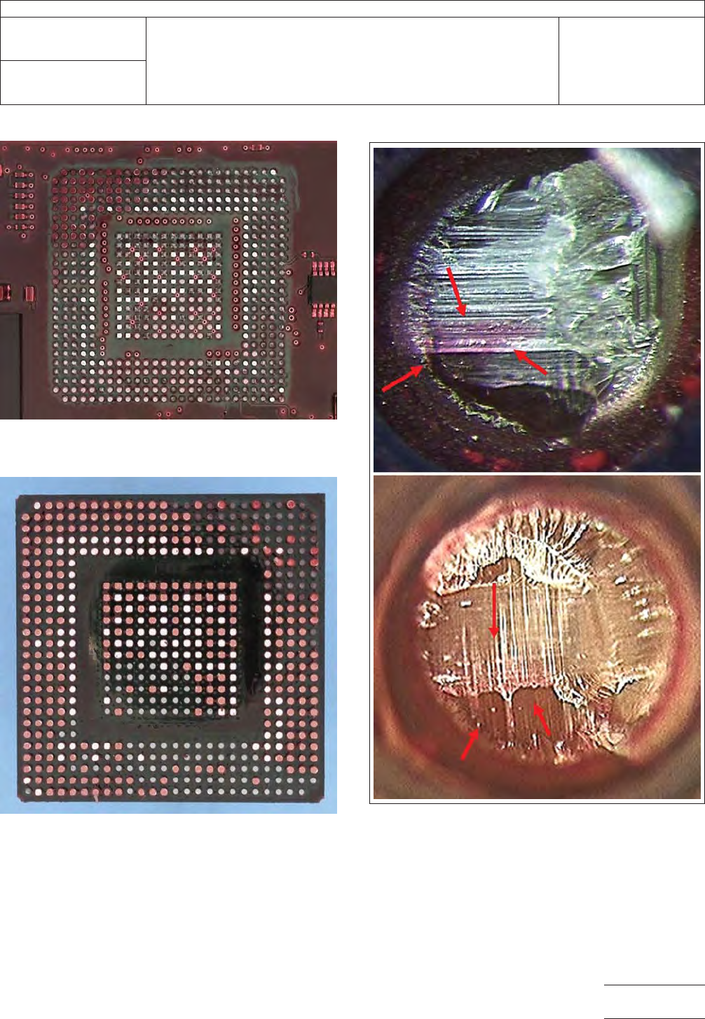
Figure 14 Mirrored Dye Indication Following Pull –
Board Side
Figure 15 Mirrored Dye Indication Following Pull –
Part Side
Figure 16 Examples of Board Showing Laminate
Fractures (Pad Cratering)
Note the faint (pink stain) red dye indication.
IPC-TM-650
Number
2.4.53
Subject
Dye and Pull Test Method (Formerly Known as Dye and Pry)
Date
8/2017
Revision
Page7of11
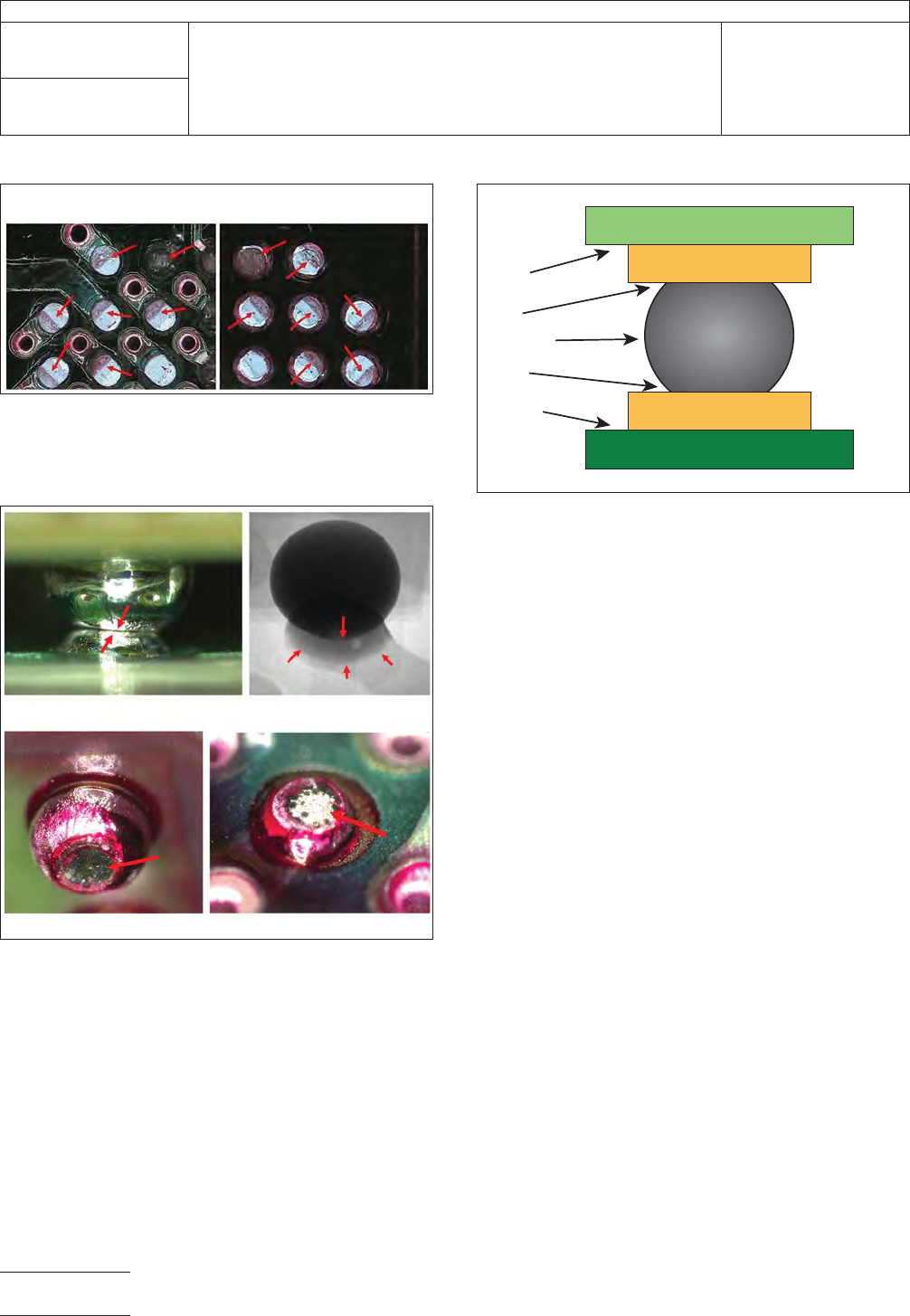
Figure 17 Example of Separation Surfaces After
Component Removal
1. Board side
2. Part side
12
Figure 18 Examples of Head on Pillow (HoP) Failures
A. Optical; IC carrier side on top and board side on bottom
B. X-ray image
C. Post dye and pull; IC carrier side
D. Post dye and pull; board side
A
B
C
D
IPC-2-4-53-19
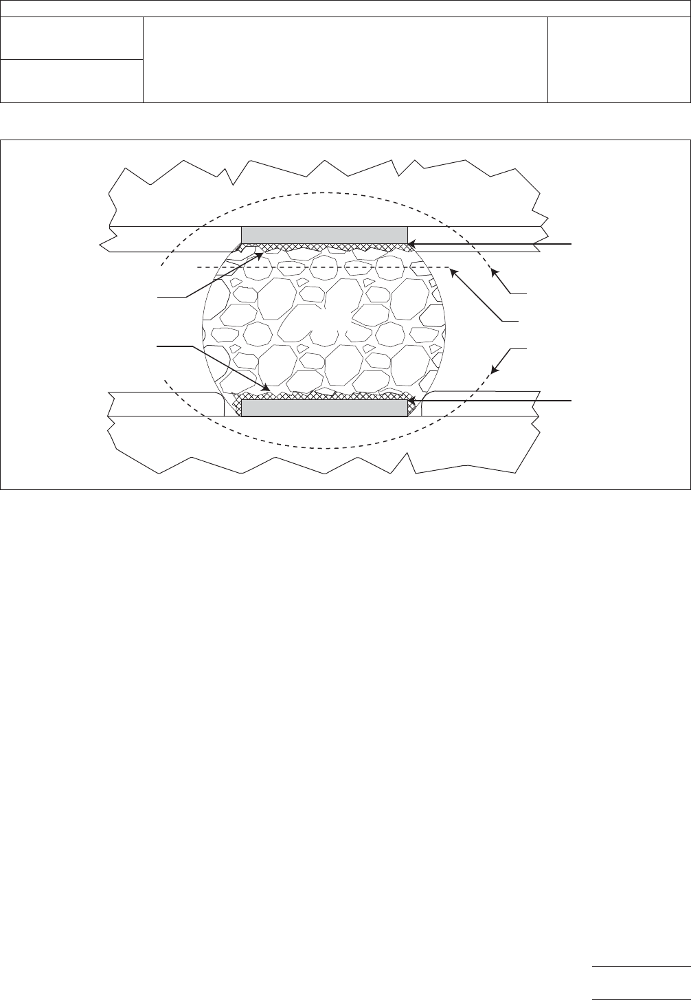
Figure 19 Example of Dye and Pull Location Type
1. Type 1X
2. Type 2X
3. Type 3X
4. Type 4X
5. Type 5X
6. BGA substrate
7. Copper pad on BGA
8. BGA solder sphere
9. Copper pad on board
10. Board laminate
1
2
5
3
6
7
9
8
10
4
IPC-TM-650
Number
2.4.53
Subject
Dye and Pull Test Method (Formerly Known as Dye and Pry)
Date
8/2017
Revision
Page8of11
IPC-2-4-53-20
Figure 20 Typical Dye and Pull Separation Locations
A. Solder ball
B. Metal pad
C. Package substrate
D. Board
E. Fracture at package side intermetallic compound (IMC)/solder interface
F. Fracture at board side IMC/solder interface
G. Fracture at package metal/IMC interface
H. Package pad lift/crater
J. Fracture within bulk solder
K. Board pad lift/crater
L. Fracture at board metal/IMC interface
A
B
C
D
E
F
G
H
J
K
L
B
IPC-TM-650
Number
2.4.53
Subject
Dye and Pull Test Method (Formerly Known as Dye and Pry)
Date
8/2017
Revision
Page9of11