IPC-TM-650 EN 2022 试验方法.pdf - 第561页
IPC-TM-650 Number Subject Date Revision where h g is the distance between the metal enclosures of the fixture; D is internal diameter of the metal enclosures; L is internal height of the metal enclosures; d r is the diam…
Number
Subject
Date Revision
Originating Task Group
Material in this Test Methods Manual was voluntarily established by Technical Committees of IPC. This material is advisory only
and its use or adaptation is entirely voluntary. IPC disclaims all liability of any kind as to the use, application, or adaptation of this
material. Users are also wholly responsible for protecting themselves against all claims or liabilities for patient infringement.
Equipment referenced is for the convenience of the user and does not imply endorsement by IPC.
3000 Lakeside Drive, Suite 105 N
Bannockburn, Illinois 60015-1249
IPC-TM-650
TEST METHODS MANUAL
1 Scope
This test method describes a way to measure the relative permittivity (
e
r
) and loss tangent (tan
d
) (also called dielectric constant,
Dk, and dissipation factor, Df) of base materials for printed boards at frequencies from 1 GHz to 20 GHz using a split post
dielectric resonator (SPDR).
2 Applicable Documents
2.1 IPC-TM-650 Method 2.5.5.2 Dielectric Constant and Dissipation Factor of Printed Wiring Board Material –
Clip Method
2.2 IPC-TM-650 Method 2.5.5.3 Permittivity (Dielectric Constant) and Loss Tangent (Dissipation Factor) of Materials
(Two Fluid Cell Method)
2.3 IPC-TM-650 Method 2.5.5.5 Stripline Test for Permittivity and Loss Tangent (Dielectric Constant and Dissipation Factor)
at X-Band
2.4 IPC-TM-650 Method 2.5.5.5.1 Stripline Test for Complex Relative Permittivity of Circuit Board Materials to 14 GHz
2.5 IPC-TM-650 Method 2.5.5.9 Permittivity and Loss Tangent, Parallel Plate, 1MHz to 1.5 GHz
3 Test Specimens
3.1 All base materials specimens shall have the metallic foil layer removed by etching or other suitable means and shall be
thoroughly cleaned. Each specimen shall be marked in the upper left corner with an engraving pencil or equivalent.
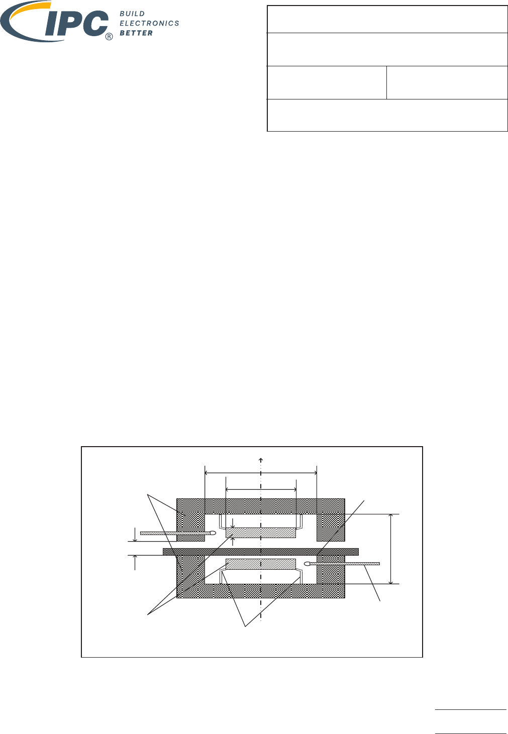
3.2 The dimensions of the test specimen shall be larger than the outer dimension of the fixture. See Figure 1.
The size of the specimen shall be larger than the internal diameter D of the metal enclosures, and the maximum thickness of the
specimen shall be smaller than the distance h
g
between the metal enclosures of the fixture.
support
coupling loop
metal enclosure
dielectric resonators
sample
D
h
g
z
h
r
L
dr
Figure 1 – Diagram of SPDR Test Fixture
Page 1 of 7
2.5.5.15
06/22 N/A
3-11a IPC-4101 Task Group
Relative Permittivity and Loss Tangent Using a
Split-Post Dielectric Resonator
IPC-TM-650
Number Subject Date
Revision
where
h
g
is the distance between the metal enclosures of the fixture;
D is internal diameter of the metal enclosures;
L is internal height of the metal enclosures;
d
r
is the diameter of the dielectric resonator;
h
r
is the thickness of the dielectric resonator.
3.3 Specimen Thickness The thicker the specimen the less error occurs in the measurements. A thin specimen may be stacked
up to a minimum of 0.4 mm [0.016 in] to improve measurement accuracy. The air gaps between the sample and the fixture do
not affect the measurement.
3.4 Number of Specimens Three specimens for the test at room temperature and one specimen for the test at variable temperatures
are required for each SPDR test fixture for this test. Table 1 shows the supported specimen dimensions
Table 1 – Specimen Dimensions
Nominal Frequency [GHz]
Specimen Sizes
mm [inch]
Maximum Thickness
mm [inch]
1 150 X 150 [5.9 X 5.9] 6.0 [0.24]
3 80 X 80 [3.2 X 3.2] 3.0 [0.12]
5 to 6 80 X 80 [3.2 X 3.2] 2.0 [0.08]
9 to 10 80 X 80 [3.2 X 3.2]
0.9 [0.035]
13 to 16 50 X 35 [2.0 X 1.4] 0.6 [0.024]
18 to 20 15 X 15 [0.6 X 0.6] 0.5 [0.020]
2.5.5.15 Relative Permittivity and Loss Tangent Using a 06/22
Split-Post Dielectric Resonator
N/A
Page 2 of 7
IPC-TM-650
Number Subject Date
Revision
Page 3 of 7
2.5.5.15 Relative Permittivity and Loss Tangent Using a 06/22
Split-Post Dielectric Resonator
N/A
4 Apparatus or Material
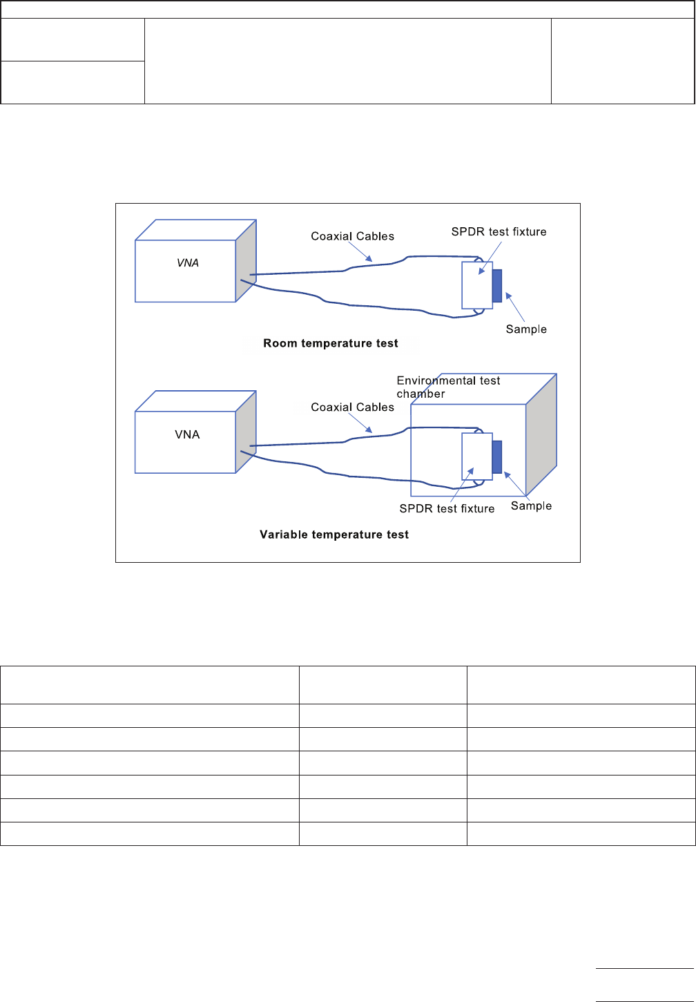
4.1 Test System The schematic diagram of the test system is shown in Figure 2. The test can be conducted at room temperature
or an elevated temperature as indicated.
Figure 2 – Schematic Diagram of Test System
4.2 Test Fixture Parameters Table 2 shows the typical relationship between the SPDR test fixture’s nominal frequency and
h
g
and D. For different test frequencies, the corresponding SPDR test fixture of nominal frequency shall be used.
Table 2 – Test Fixture Configurations
SPDR Test Frequency
[GHz]
D
mm [inch]
hg
mm [inch]
1 120 [4.7] 6.0 [0.24]
3 50 [2.0] 3.0 [0.12]
5 to 6 30 [1.2] 2.0 [0.08]
9 to 10 22 [0.9] 0.9 [0.035]
13 to 16 15 [0.6] 0.6 [0.024]
18 to 20 10 [0.4] 0.5 [0.020]
4.3 Vector Network Analyzer (VNA) The frequency range of the VNA shall be 500 MHz to 20 GHz, The dynamic range of the
VNA shall be more than 60 dB.
4.4 Calibration Reference The calibration equipment shall include a standard reference sample. For example, a single-crystal
quartz or equivalent reference, and a calibration assembly for the VNA.