IPC-TM-650 EN 2022 试验方法.pdf - 第553页
It is important to note that these are just footprint examples, and the electrical performance of these footprint may be fur- ther improved based on the layer stackup, such as voiding the ground plane right beneath the s…
structure are measured first. Assuming the 2X-Thru structure
is symmetric, the S-parameters of a 1X structure can be cal-
culated directly from the 2X-Thru measurement. Once the
S-parameters of the 1X structure on both sides on the DUT
are obtained, the S-parameters of the DUT can be readily cal-
culated. This significantly simplifies calibration/de-embedding
procedures as compared to a traditional TRL calibration
where six calibration structures are typically needed.
There are various 2X-Thru de-embedding tools available at
time of publication of this test method, such as [9][10][11]. The
accuracy of 2X-Thru de-embedding tool is has been shown to
be comparable to TRL [13]. However, since the algorithm of
commercially available 2X-Thru methods are often proprietary,
it is up to the users to validate the tool for their printed board
insertion loss measurements. IEEE 370-2020 addressing this
issue by setting up a process to validate the de-embedding
tools [12]. Below is the general process of using 2X-Thru
de-embedding process to measure the insertion loss:
1) Manufacture two printed board conductors with different
lengths (L1 and L2).
2) Perform SOLT calibration to move reference plane to the
end of coaxial connector.
3) Perform VNA measurement and to acquire the S param-
eters of the shorter conductor (L1) and longer trace (L2).
4) Use 2X-Thru tool to de-embed the S parameters of L2,
while treating the shorter conductor L1 as test fixture. This
end up with S parameters of a transmission line DUT of
length L2-L1.
5) Renormalize the S parameter using the characteristic
impedance of transmission line.
6) The renormalized S21 represents the insertion loss of DUT
(length of L2-L1).
2 Applicable Documents
IPC-TM-650
Test Methods Manual
2.5.5.12 Test Methods to Determine the Amount of Signal
Loss on Printed Boards
3 Test Specimens
3.1 Common Test Coupon Characteristics
The test
coupon contains two or more transmission lines. The follow-
ing are general guidelines for designing transmission line test
structures for the test methods within this document. These
transmission line test structures may be placed within the
functional area of the printed board or within test coupons. It
is recommended that coupons have labels that contain infor-
mation about the associated test line signal layer; for example,
L1, L3, etc. Labeling of the contact land for differential
conductors shall clearly indicate the matched pair. It is recom-
mended that test coupons include a printed board serial num-
ber, part number, and date code.
3.2 Ground and Reference Planes All reference planes in
the coupon shall be connected together within the coupon
area and be independent of those planes in the functional cir-
cuit area.
3.3 Probe Launch Footprint The probe launch footprint is
comprised of signal pads and ground contact. Each probe
vendor can specify its optimized probe launch footprint. How-
ever, it is desirable to have footprint that is compatible with
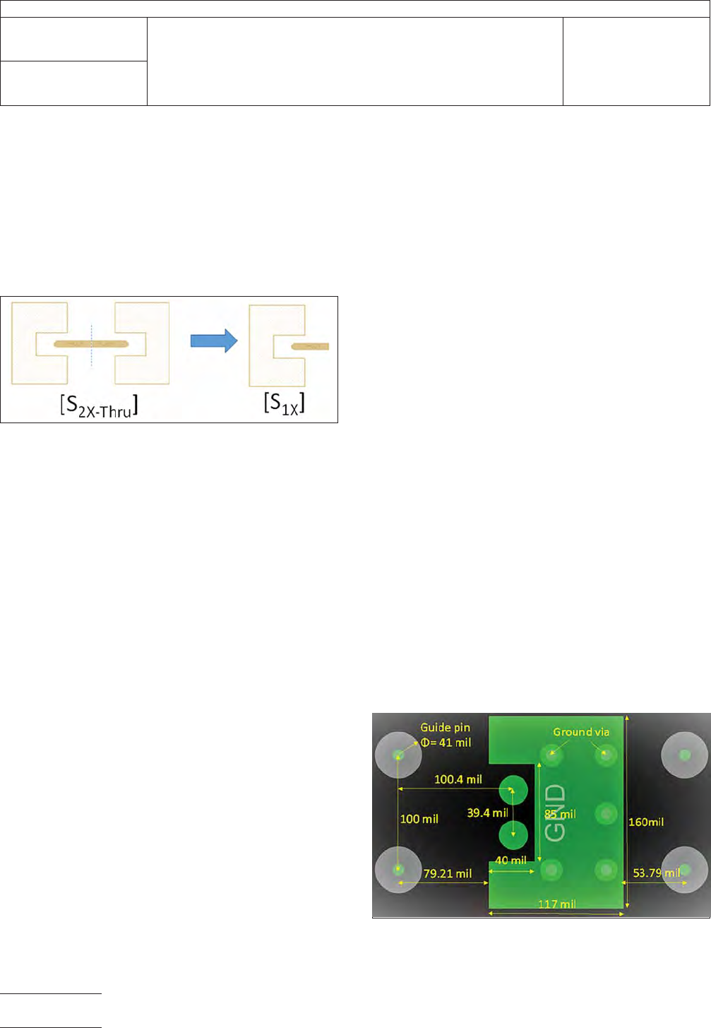
multiple probes. Figure 3-1 shows an example of a differential
probe launch footprint compatible with both micro- and hand-
held probes. A similar single-ended probe launch footprint is
shown in Figure 3-2, with the same guide pin design.
IPC-25514-1-5
Figure 1-5 S parameter of Test Fixture is Calculated from
S Parameter of 2X-Thru
IPC-25514-3-1
Figure 3-1 Example of a Probe Launch Footprint for
Differential Signal Probing (both footprint and dimensions
are shown for informative purposes only)
IPC-TM-650
Number
2.5.5.14
Subject
Measuring High Frequency Signal Loss and Propagation on
Printed Boards with Frequency Domain Methods
Date
02/2021
Revision
Page4of11
It is important to note that these are just footprint examples,
and the electrical performance of these footprint may be fur-
ther improved based on the layer stackup, such as voiding the
ground plane right beneath the signal pads. Each probe ven-
dor can specify its optimized probe launch footprint that
meets the electrical requirement specified in 4.2. Furthermore,
it is critical to work with probe vendor to make sure the fin-
ished drill hole size is compatible with the probe.
Note that the footprint example shown in Figure 3-1 is appli-
cable for measurements up to 20GHz and that the footprint
can be further optimized for application at higher frequencies.
3.4 Connector Launch Alternative to microwave probes,
high bandwidth connector launch may be used instead of
probe launch as show in Figure 3-2 and Figure 3-3 of IPC-
TM-650 Method 2.2.2.12A. Although the hand-held probe
approach is quicker and more convenient to use, the connec-
tor solution is usually more reliable and less prone to human
errors.
3.5 General Surface Condition The panel test coupons
shall have the same surface plating and use the same solder
mask requirements as the functional printed board. The plat-
ing of the launch footprint should be suitable for probing or
co-axial connector connection.
3.6 General Routing Guidelines The test lines shall be
referenced to a continuous ground/voltage planes. The test
line conductors shall be kept at minimum distance Dmin from
printed board structures such as voids, plane splits, other
conductors and holes, where Dmin is six times the height of
dielectric layer (from line conductor to the closest reference
plane) or 2.54 mm [0.100 in], whichever is greater.
Fiber-weave impact should be mitigated unless the intent is to
measure its impact. One mitigation example is to have the test
line routed at about 10 degree angle (or close to the routing
scenario in actual product design) with respect to the fiber-
weave alignment. Alternative, straight routing (parallel to board
edge) can be used if the Gerber image is rotated by about 10
degrees on the panel.
It is recommended to route the test lines with the same cross-
section and target impedance as in the actual product layout.
Thieving, which is the use of non-terminated copper struc-
tures such as planes, pads, and/or conductors adjacent to
test lines that ensure plating consistency, may be used on the
test coupon. All thieving structures (if used) shall be placed at
least Dmin away from each test interconnect. It is recom-
mended to make sure copper density at each routing layer is
representative of the actual product.
3.7 Impact of Vias in the Printed Board Conductor Loss
Characterization
Measuring the signal loss for inner layer
(stripline) can be challenging when there is a substantial loss
due to the via or via stub effect. Reducing via effect can
improve the de-embedding results. This can be achieved by:
• Minimizing via stub length by probing from the appropriate
side of the board (from the top for traces on the bottom half
of the board and vice-versa, to assure minimum via stub
length)
• Minimizing via stub length by back-drilling. However, this
needs to be done with good control of back-drilling depth.
Inconsistent back-drilling depth between the vias for two
different routing length can lead to large de-embedding error
• Extra attention needs to be paid to stacked via designs, as
this approach, while avoiding stubs and improving signal
integrity, has high manufacturing variants
• The resonance frequency should be outside of intended
measurement bandwidth
For signals on outer layer (microstrip), the conductor should
be routed without via or via stub.
3.8 Impact of Environmental Condition in the Printed
Board Conductor Loss Characterization
Temperature
and humidity affect loss measurements. It is therefore critical
to clearly document the testing condition in the reported inser-
tion loss.
For insertion loss of conductors routed on outer layer, the
results can be different under the conditions described in
3.8.1 vs. those described in 3.8.2 due to the humidity impact.
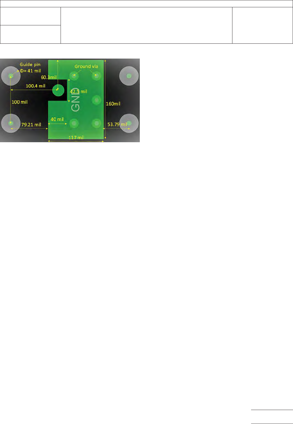
IPC-25514-3-2
Figure 3-2 Example of a Probe Launch Footprint
for Single-ended Signal Probing (both footprint and
dimensions are shown for informative purposes only)
IPC-TM-650
Number
2.5.5.14
Subject
Measuring High Frequency Signal Loss and Propagation on
Printed Boards with Frequency Domain Methods
Date
02/2021
Revision
Page5of11
As the solid metal planes may block the moisture penetration,
for the conductors routed on inner layers it typically takes a
long time (with rare exceptions) for the sample to absorb the
moisture. Therefore, making measurement of insertion loss of
inner routing layers under the conditions described in 3.8.1 is
recommended over making such measurements under the
conditions described in 3.8.2.
3.8.1 Insertion Loss Measurement of Vacuumized Test
Specimens
Test specimens can be vacuumized right after
baking them at 105 °C RH 0% over 2 hours, or 140 °C RH
0% over 1 hour. However, if the coupon has been stored over
a long period of time without proper vacuum packaging, the
baking condition needs to be adjusted to be 140 °C RH 0%
for 12 hours. Consistent results can be obtained by testing
specimens at 23 °C (± 2 °C) [73.4 °F (± 3.6 °F)] and 20~80%
RH for less than 12 hours since opening the vacuum package
or finishing a baking treatment. It is recommended to allow
test coupons to cool to room temperature for at least 30 min-
utes before test if measurement is done after a baking treat-
ment.
3.8.2 Insertion Loss Measurement of Test Specimens
Stored in Environmental Chamber
For conductors routed
on outer layers, consistent results of insertion loss at typical
humidity condition can also be obtained by storing test speci-
mens at 23 °C (± 2 °C) [73.4 °F (± 3.6 °F)] and 40% RH (± 5%
RH) for no less than 48 hours. Note that the test under this
condition takes longer time compared to that described in
3.8.1.
4 Apparatus
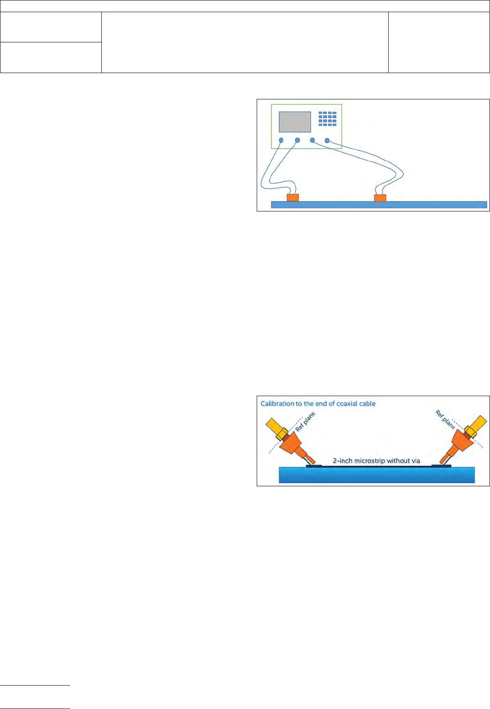
4.1 VNA Measurement Apparatus
The measurement
equipment needed includes a VNA, calibration kit, cabling,
and a probing solution, as shown in Figure 4-1. High perfor-
mance connectors and cables that are rated above the maxi-
mum frequency of interest are required in performing VNA
measurements.
Using TDR/TDT system in place of a VNA to acquire fre-
quency domain attenuation and loss data is beyond the scope
of this test method. A future IPC-TM-650 Test Method
2.5.5.15 for best design practices for Time Domain method is
envisioned under the IPC D-24D Task Group.
4.2 Probe Quality The quality of probe (whether using
probing station or handheld probe) is critical for accurate and
repeatable measurement. It is recommended to have the
insertion loss of the probe and launching pad to be less than
3.5 dB at highest frequency of interest, to make sure the
probe and launching pad design have good electrical perfor-
mance.
A direct measurement of electrical performance of probe and
launching pad can be cumbersome. Alternatively, Figure 4-2
shows an example of test setup to check the electrical perfor-
mance. A 50.8 mm [2.0 in] microstrip line with known insertion
loss is used to provide a connection between two probes.
VNA is calibrated to the end of coaxial cable, and the inser-
tion loss of the 50.8 mm [2.0 in] microstrip line with probes at
both ends is measured.
Insertion loss requirement for the test setup in Figure 4-2
depends on the highest measurement frequency, as well as
the microstrip trace loss. A test coupon with known loss can
be used, or a separate measurement can be done to deter-
mine microstrip loss. Figure 4-3 shows an example of the
probe quality requirement, assuming the highest measure-
ment frequency is 20 GHz, and the insertion loss of the
50.8 mm [2.0 in] microstrip is 5 dB at 20 GHz. The measured
insertion loss must be above the red dash line in the figure.
Note at DC level, the required loss is less than 1 dB, and at
20 GHz, the required loss is less than12 dB (where 3.5 dB is
allocated for each probe, and 5 dB is coming from the
50.8 mm [2.0 in] microstrip).
IPC-25514-4-1
Figure 4-1 Typical VNA Measurement Setup
IPC-25514-4-2
Figure 4-2 Test Setup for Probe Quality Check
IPC-TM-650
Number
2.5.5.14
Subject
Measuring High Frequency Signal Loss and Propagation on
Printed Boards with Frequency Domain Methods
Date
02/2021
Revision
Page6of11