IPC-TM-650 EN 2022 试验方法.pdf - 第419页
IPC-TM-650 Number Subject Date Revision Page 7 of 7 2.4.54 Test Method for Thermal Transmission Properties of 09/2022 Metal Based Printed Boards (MBPB) N/A 6 Notes 6.1 The following information should be given in the mea…
IPC-TM-650
Number Subject Date
Revision
Page 6 of 7
2.4.54 Test Method for Thermal Transmission Properties of 09/2022
Metal Based Printed Boards (MBPB)
N/A
Equation 14). With the thickness from the microsection it is possible
to calculate the apparent thermal conductivity of the dielectric
layer (Table 1 Equation 16). This calculated value must be shown
in the measurement report including the dimensions (mm²K/W)
(Table 1 Equation 15) as well as the apparent thermal conductivity
in W/(mK) (Table 1 Equation 16) and the thicknesses in µm.
5.10 Measure three identical samples across the board and list
all results in the measurement report. In addition, the mean value
and the standard deviation must be listed as well in the report.
5.11 To measure the DIE thickness a cross section according to
IPC-TM-650 Test Method 2.1.1 should to be made.
5.12 To embed the sample, the specimen is first cut in half using
a e.g., metal saw. Afterwards the specimen gets embedded,
grinded and polished.
5.13 The thicknesses of the top and dielectric layer are measured
in the microsection on five different points using a microscope.
Calculate the middle value of the five measured values for each
layer. From the total thickness of the sample, the thickness of
the base layer can be determined by subtraction (see Table 1
Equation 17).
1
2
3
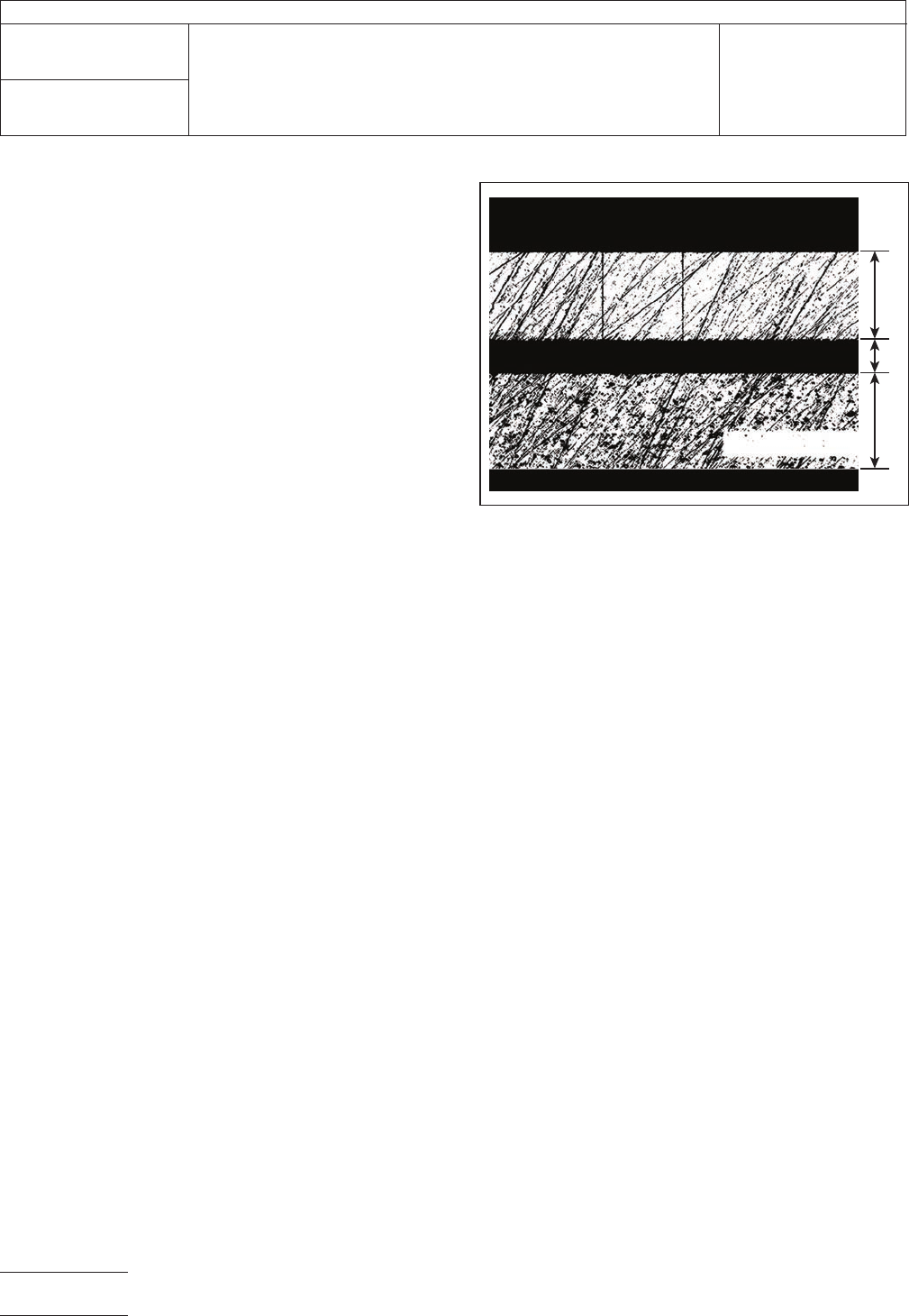
Figure 5 Layer Structure of a Metal-Based Board
Note 1: Top layer: d
top,
see 1.3.1
Note 2: Dielectric layer: d
die
Note 3: Base layer: d
base

IPC-TM-650
Number Subject Date
Revision
Page 7 of 7
2.4.54 Test Method for Thermal Transmission Properties of 09/2022
Metal Based Printed Boards (MBPB)
N/A
6 Notes
6.1
The following information should be given in the measurement report associated with the measurement. Show all measured
values and the mean value for all parameters:
6.2 General information:
6.2.1 Measurement institution
6.2.2 Testing apparatus (identification)
6.2.3 Date
6.2.4 Contact person
6.3 Specimen identification:
6.3.1 Name of the manufacturer
6.3.2 Batch or lot number
6.3.3 Grade designation
6.3.4 Nominal thickness
6.3.5 Any other information pertinent to the identification of the material
6.4 Results and thermal properties
6.4.1 Number of layers used in the test
6.4.2 Average temperature of the specimen (@ max pressure)
6.4.3 Temperature difference over the specimen (@ max pressure)
6.4.4 Pressure used during testing
6.4.5 Apparent thermal conductivity (@ max pressure)
6.4.6 Thermal resistance (@ max pressure)
6.4.7 Uncertainty of the thermal measurement (@ max pressure)
6.4.8 Layer thicknesses of top, base and dielectric layer
6.4.9 Microscopic images of the layer thicknesses
6.4.10 Used material to reduce contact resistances between meter bars and specimen
6.4.11 Assumptions of the thermal conductivity of the top and base plate to determine the thermal properties of the dielectric
layer
6.4.12 Determined thermal conductivity of the dielectric layer (@ max pressure)
6.5 The following information show how to use the values from this method for CFD simulation.
Build up a three-layer system in your simulation tool according to Figure 5. Use for upper and lower metal layer the mean value
of the thickness from microsection and the thermal conductivity of each metal layer. Use the mean value of apparent thermal
conductivity (Table 1 Equation 16) and thickness of the dielectric material.

1.0
Scope
This
method describes a technique for evaluat-
ing a material to resist tracking when subjected to a low cur-
rent arc just above the surface of the material. It can be used
on materials of various thickness by stacking materials. This
procedure is based on techniques described in ASTM D495.
2.0
Applicable Documents
ASTM D495
Standard
Test Method for High Voltage, Low-
Current, Dry Arc Resistance of Solid Electrical
Insulation
Manufacturer’s Instruction Manual
3.0
Test Specimens
3.1 Number
Three
specimens shall be used unless other-
wise specified.
3.2
Form
Each
specimen shall be 3.0 in. x 2.0 in. Material
under 0.06 in. in thickness shall be built up to provide a speci-
men at least 0.06 in. but not exceeding 0.125 in. For very thin
laminates a 1/16 in. laminate of the same type may be used
under the actual specimen subjected to the arc, permitting a
reduction of the material required without significantly affecting
the results.
3.3
Location
Specimens
may be cut from any location in a
sheet (except from the outer 1 in. of full size sheets).
3.4
Foil Clad Materials
All
foil clad materials shall have the
foil removed by etching and shall be thoroughly cleaned prior
to conditioning or testing.
4.0
Apparatus/Materials
4.1
Arc
tester (Beckman ART-1
1
or
equivalent, see ASTM
D495).
4.2
Tungsten
electrodes (Beckman
2
or
equivalent, see
ASTM D495).
4.3
Constant
temperature water bath capable of 50°C ±
2°C, filled with distilled water.
4.4
Beaker
or pan filled with ambient temperature distilled
water.
4.5
Racks
for supporting specimens in the water bath with
all surfaces exposed.
4.6
Shear,
saw or paper cutter for cutting specimen.
4.7
Alcohol
or other solvent for cleaning electrode.
4.8
Crocus
cloth.
4.9
Gage
blocks for checking electrode spacing 0.248 in.
and 0.252 in.
4.10
Lint
free paper towels.
4.11
Variac
3
autotransformer
type W1OMT or equivalent.
5.0
Procedure
5.1 Preconditioning
Unless
otherwise specified the speci-
mens shall be conditioned for 48 hours (± 2 hours -0 hours) in
distilled water maintained at 50°C ± 2°C. Following this step
the specimens shall be immersed in ambient temperature dis-
tilled water for 30 minutes minimum, 4 hours maximum, to
allow them to reach temperature equilibrium without loss of
moisture.
5.2
Test Conditions
The
test shall be run at ambient tem-
perature 23°C ± 5°C and ambient humidity.
5.3
Equipment set up
5.3.1
The
electrode assembly shall be cleaned thoroughly
using alcohol or other suitable solvent and, if required, with
crocus cloth. The electrode gap shall be adjusted if necessary
to provide a gap of 0.250 in. ± 0.002 in. when the electrodes
1.
ART-1 or ART-2 manufactured by Beckman Instruments Cedar Grove Essex County New Jersey, U.S.A.
2. Electrodes manufactured by Beckman Instruments
3. Variac available from General Radio
The
Institute for Interconnecting and Packaging Electronic Circuits
2215 Sanders Road • Northbrook, IL 60062
IPC-TM-650
TEST
METHODS MANUAL
Number
2.5.1
Subject
Arc
Resistance of Printed Wiring Material
Date
5/86
Revision
B
Originating Task Group
N/A
Material
in this Test Methods Manual was voluntarily established by Technical Committees of the IPC. This material is advisory only
and its use or adaptation is entirely voluntary. IPC disclaims all liability of any kind as to the use, application, or adaptation of this
material. Users are also wholly responsible for protecting themselves against all claims or liabilities for patent infringement.
Equipment referenced is for the convenience of the user and does not imply endorsement by the IPC.
P
age1of2
电子技术应用 www.ChinaAET.com