IPC-TM-650 EN 2022 试验方法.pdf - 第106页
5.1.3 To standardize measurements, use test structures in whic hb=1 8µ m ,c= 63.5 µm, and the ratio of c/b is 3.5 ± 0.2. If a dielectric film is used, which has been produced at a fixed thickness other than that outlined…
all
steps recommended for full curing. For resin coated cop-
per (RCC) foil, after laminating the foil, cure as per manufac-
turer’s instructions, then etch the copper layer and proceed
as for other deposited dielectric materials (see Figure 3).
4
Equipment/Apparatus
This
method uses profilometer
measurements providing topological height variations as a
function of displacement across the surface of a standard test
structure.
Use a TENCOR Profilometer (Model: Alpha Step 200). Substi-
tutions are acceptable, provided they can measure feature
heights in the range used to within ± 2% and can provide a
linear scan of at least 10 mm.
Note:
As
an alternate method, where a profilometer is not
available, the measurements can be collected by cross-
sectioning the test structures. This method will require one
cross-section for each trace width in order to collect data for
trace width effects.
5
Procedure
Prior
to the polymer deposition, scan the pro-
filometer stylus across all copper lines in the test structure,
scanning in the direction indicated by the arrow in Figure 2.
Measure and record the dimensions depicted as ‘‘a’’ and ‘‘b’’
in Figure 1 for each of the lines.
After polymer deposition and cure, measure the polymer film
thickness at a location distant (at least 15 line widths) from any
of the test structure’s copper lines. In order to do this, a ‘‘win-
dow’’ must be imaged in the dielectric down to the substrate.
A ‘‘window’’ to the substrate may be opened by photo-
imaging, chemical dissolution, laser ablation, or other appro-
priate method (see Figure 4). The sweep must allow measure-
ments of the thickness of the dielectric entering and exiting
the ‘‘window.’’ These measurements should be within ± 0.2
µm of each other. Record this dielectric thickness as dimen-
sion ‘‘c.’’
Finally, measure the dimension shown in Figure 1 as the fea-
ture step height ‘‘d’’ of the polymer; use the profilometer, not
an optical method. In measuring ‘‘d,’’ take the difference in
height between the highest point on top of the copper line and
the lowest point at least 15 line widths from the line to be
measured.
5.1
Conditions of Test
5.1.1
Calibrate
the profilometer before making measure-
ments using the calibration procedure specified by the manu-
facturer of the equipment.
5.1.2
Measure
at ambient room temperature and humidity.
IPC-2-2-21-3
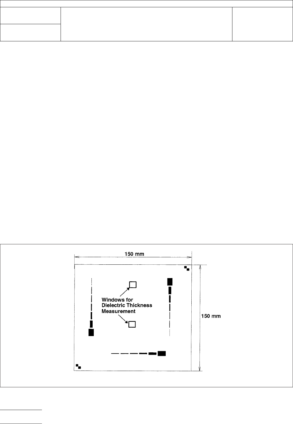
Figure
3 Pattern of One Test Board Showing Three Test Substructures (Board is 150 mm sq.)
IPC-TM-650
Number
2.2.21
Subject
Planarity
of Dielectrics for High Density Interconnection (HDI)/
Microvia Technology
Date
11/98
Revision
P
age2of4
电子技术应用 www.ChinaAET.com
5.1.3 To
standardize measurements, use test structures in
whichb=18µm,c=63.5 µm, and the ratio of c/b is 3.5 ±
0.2. If a dielectric film is used, which has been produced at a
fixed thickness other than that outlined above, maintain a c/b
ratio as described. If the standard construction with this
defined ratio cannot be maintained, the actual metal and
dielectric thickness must be reported.
5.1.4 Make
triplicate measurements and average the results
at each line width.
5.2
Calculation of Planarity
5.2.1
Planarity
for an individual trace, P
a
,
can be defined by
the following equation:
P
a
=
(1 - d/b)100
where ‘‘a’’ is the trace width, ‘‘d’’ is the bump height over the
trace, and ‘‘b’’ is the copper trace height. For an ideal planar
structure, the value of P is equal to 100%.
5.2.2
Average
planarity, P
ave
,
for a given trace width is cal-
culated using the triplicate measurements:
P
ave
=(P
a1
+P
a2
+P
a3
)/3
5.2.3
Total average planarity, P
total
, is the average planarity
for all widths of traces (where n = number of traces widths
measured):
P
total
=(
P
ave1
+P
ave2
+
.......+ P
ave
n
)/n
5.3
Report
5.3.1
Report
the average planarity for each trace width
measured (see 5.2.2).
5.3.2
Report
the total average planarity as a single average
percentage of all seven trace width averages (see 5.2.3).
5.3.3
Also
report the technique, profilometer or cross-
section, used to obtain the measurements.
This calculation can be performed for each trace width to
develop a planarity plot.
6 Notes
6.1
Cross Section Method
Due
to the field of view
required for the larger trace widths (> 0.8 mm), accurate mea-
surements of the dielectric ‘‘bump’’ may not be possible due
to the low magnification. One option is to use a higher mag-
nification and measure the total dielectric and copper trace
height from the substrate surface and subtract the minimum
dielectric height over the substrate alone.
6.1
Planarity Test Method Sample
An
example of a pla-
narity test method is given in Figure 5.
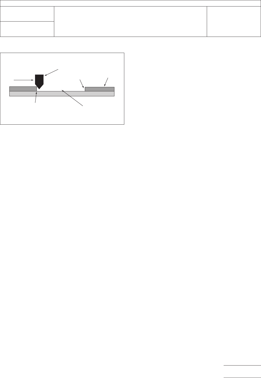
IPC-2-2-21-4
Figure
4 Cross Section of Window Used for Dielectric
Thickness Measurement
Pr
ofilometer Stylus
Direction
of Scan
Height at Exit
Dielectric
Height at Entry
``Window´´ in Dielectric
IPC-TM-650
Number
2.2.21
Subject
Planarity
of Dielectrics for High Density Interconnection (HDI)/
Microvia Technology
Date
11/98
Revision
P
age3of4
电子技术应用 www.ChinaAET.com
IPC-2-2-21-5
Figure
5 Planarity Chart for Method.xls
6.4
3.2
1.60.8
0.40.2
0.1
0.0
10.0
20.0
30.0
40.0
50.0
60.0
70.0
80.0
90.0
100.0
T
race Width (mm)
Planarity Test Method - Sample A
Pr
ofilometer Method A
% Planarity
X-Section Method A
IPC-TM-650
Number
2.2.21
Subject
Planarity
of Dielectrics for High Density Interconnection (HDI)/
Microvia Technology
Date
11/98
Revision
P
age4of4
电子技术应用 www.ChinaAET.com