IPC-TM-650 EN 2022 试验方法.pdf - 第799页
1.0 Scope 1.1 To determine the effects of exposing connectors to extremes of high and low temperature and of the mechanical stresses created by rapid transition between the temperature extremes. 2.0 Reference Documents 2…
5.3 The solder bath shall be occasionally stirred with a clean
stainless steel paddle to ensure that it is of uniform composi-
tion and temperature throughout. The surface of the bath shall
be skimmed immediately prior to each test to remove any
dross or residual unburned flux from previous tests.
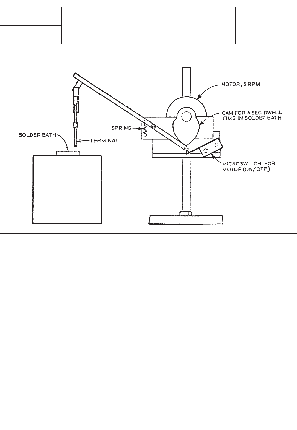
5.4 The sample shall be affixed to the dipping device shown
in Figure 2 and oriented so that the contact termination will
enter the solder bath to the specified depth.
5.5 The sample shall be immersed in the solder bath at a
rate of 1.00 ± 0.25 inches per second and withdrawn at the
same rate. The dwell time in the solder shall be 5.0 ± 0.5 sec-
onds.
5.6 The sample shall not be removed from the dipping
device or otherwise disturbed until the solder has solidified.
5.7 The sample shall be thoroughly cleaned of residual flux
and examined under 10X magnification for evidence of the
following:
A. Dewetting of areas to be soldered.
B. Pinholes or voids in the solder coat.
C. Incomplete fill of solder well or hole.
6.0 Notes
6.1
Acceptance criteria shall be established in terms of one,
or any combination, of the following:
A. Less than 95% coverage of flat surfaces.
B. Pinholes or small voids or solder surface roughness con-
centrated in any one area of the contact.
C. Poor filleting around wire or incomplete fill of solder well.
IPC-3-10-2
Figure 2 Suggested Dipping Device for Solderability Test
IPC-TM-650
Number
3.10
Subject
Solderability, Connectors
Date
7/75
Revision
A
Page2of2
1.0 Scope
1.1
To determine the effects of exposing connectors to
extremes of high and low temperature and of the mechanical
stresses created by rapid transition between the temperature
extremes.
2.0 Reference Documents
2.1
Information in this section is intended to parallel the test
method described in EIA-RS-364/TP-32.
3.0 Test Specimen
3.1
A connector (plug and receptacle) complete with all
applicable guide, keying and engaging hardware or a card-
edge receptacle.
3.2 The plug and receptacle shall be tested in a configura-
tion normal to its functional capacity including mounting, ter-
mination, and mating.
3.3 The plug and receptacle or the card-edge receptacle
and a nominal thickness printed circuit board shall be mated
during this test, except as otherwise specified.
4.0 Apparatus
4.1
A dual chamber (or two separate chambers) capable of
maintaining the applicable temperature within ± 2°C at the
geometric center under no load conditions, and a thermal dis-
tribution not greater than ± 5°C of the temperature at the
geometrical center.
5.0 Procedure
5.1
The chamber(s) shall be adjusted to, and maintained at,
the high and low extremes specified in the individual connec-
tor specification. Thermal equilibrium shall be attained prior to
the start of the test. (See 6.3)
5.2 The mated test specimen shall be suspended within the
low temperature chamber and subjected to the number of
continuous thermal shock cycles specified in the individual
connector specification. One complete cycle of thermal shock
is defined by Table 1. (See 6.4)
Table 1 Thermal Shock Test Conditions (One Cycle)
Step Temperature, °C Time
1 Low extreme (+0, -5°C) 30 min. (min.)
2 25°C (+10, -5°C) 2 min. (max.)
3 High extreme (+5, -0°C) 30 Min. (min.)
4 25°C (+10, -5°C) 2 min. (max.)
WARNING:
BOTH THE HIGH AND LOW TEMPERATURE
EXTREMES USED DURING THIS TEST WILL CAUSE
SEVERE BURNS. USE INSULATED GLOVES WHEN HAN-
DLING THE TEST SPECIMEN.
5.3 After completion of the specified number of cycles and
attaining room ambient temperature, the sample shall be visu-
ally examined for evidence of the following:
A. Excessive permanent dimensional changes (distortion).
B. Cracking or delamination of finishes or dielectric materials.
C. Opening of seals or seams.
D. Hardening or softening of dielectric materials.
5.4 Unless otherwise specified in the individual connector
specification, the test specimen shall be subjected to the with-
standing voltage test, (3.13).
6.0
Notes
6.1 Acceptance criteria shall be established in terms of one,
or any combination, of the following:
A. Visible evidence of damage or significant material change.
B. A deterioration in withstanding voltage occasioned by
internal fissures in the dielectric with or without the
accompanying entrapment, of moisture.
6.2 The test chambers shall be of the forced (circulating) air
type to insure even temperature distribution.
2215 Sanders Road
Northbrook, IL 60062-6135
IPC-TM-650
TEST METHODS MANUAL
Number
3.11
Subject
Thermal Shock, Connectors
Date
7/75
Revision
A
Originating Task Group
N/A
Material in this Test Methods Manual was voluntarily established by Technical Committees of the IPC. This material is advisory only
and its use or adaptation is entirely voluntary. IPC disclaims all liability of any kind as to the use, application, or adaptation of this
material. Users are also wholly responsible for protecting themselves against all claims or liabilities for patent infringement.
Equipment referenced is for the convenience of the user and does not imply endorsement by the IPC.
Page1of2
ASSOCIATION CONNECTING
ELECTRONICS INDUSTRIES

6.3 Thermal equilibrium shall be assumed to have been
attained when three successive temperature readings taken at
five-minute intervals show a variation not greater than 3°C.
6.4 The exposure and transfer times specified in Table 1 are
based on an assumed sample weight less than 0.5 pound
(226 GMS). Appropriate increases in these periods shall be
made for larger samples to ensure that the designated test
temperature is attained.
IPC-TM-650
Number
3.11
Subject
Thermal Shock, Connectors
Date
7/75
Revision
A
Page2of2