IPC-TM-650 EN 2022 试验方法.pdf - 第306页
1.0 Scope This test method establishes a procedure for determining the flatness of silicon wafers coated with depos- ited organic films. 2.0 Applicable Documents ASTM D 618 Standard Practice for Conditioning Plastics and…

5.3
Calculation of Results
5.3.1 Average Bow and Twist Results
Bow and Twist =
Sum of the Measured Maximum
Vertical Displacements in mm [in]
Number
of Test Specimens
5.3.2
Maximum Bow and Twist Results
The
maximum
vertical displacement in mm [in] obtained for each lot of
material.
6.0 Notes
6.1
This
is the referee method; other methods of measure-
ment are allowable, if agreed upon between user and vendor.
IPC-TM-650
Number
2.4.22.1
Subject
Bow
and Twist—Laminate
Date
5/93
Revision
C
P
age2of2
电子技术应用 www.ChinaAET.com

1.0
Scope
This
test method establishes a procedure for
determining the flatness of silicon wafers coated with depos-
ited organic films.
2.0
Applicable Documents
ASTM D 618
Standard
Practice for Conditioning Plastics and
Electrical Insulating Materials for Testing
3.0
Test Specimen
The
test specimens are 125 mm diam-
eter silicon wafers 625 ± 15 µm in thickness. The surface of
the wafers must be clean, and at least one side of the wafers
must be polished. A minimum of 9 wafers are required.
4.0
Apparatus or Material
4.1 Radius Of Curvature Measurement Device
Flexus
Thin
Film Stress Measuring Apparatus (TFSMA) Model 2-300
or equivalent.
4.2
Wafer Thickness Measurement Device
Micrometer
capable
of measuring accurately to 5 µm. A thickness gauge
including weights can also be purchased from Flexus that can
be used with the TFSMA to measure thickness.
4.3
Film Thickness Measurement Device
Nanospec
Model
210, Tencor AlphaStep, or equivalent film thickness
measurement device capable of measuring accurately to 0.1
µm.
5.0
Procedure
5.1 Radius Of Curvature Of Uncoated Wafers
5.1.1
Label
each wafer with a unique identification.
5.1.2
Measure
the thickness of the uncoated silicon wafers.
5.1.3
Measure
the radius of curvature of the uncoated
wafers following the manufacturers recommended procedure.
5.2
Coat Wafers
5.2.1
Use
a minimum of three film thicknesses for each
polymer or processing condition investigated. The film thick-
nesses should span as large a range as possible, e.g., 5, 10
and 15 µm. Coat at least three wafers for each film thickness
for a minimum of nine wafers.
5.2.2 Coat
the polymer solution onto the back (unpolished
side) of the silicon wafers using manufacturer s recommended
deposition technique (e.g., spin coating). Process the coating
according to the manufacturer s recommended procedures.
The final film thickness must not vary by more than 2% across
the substrate surface.
5.3
Radius of Curvature Of Coated Wafers
5.3.1
The
coated wafers should be conditioned at 23 ± 2°C
and 50 ± 5% relative humidity for exactly 24 hours prior to
testing. Many polymers exhibit stress relaxation or a decrease
in stress associated with moisture absorption, therefore it is
essential that the coated wafers are equilibrated under identi-
cal conditions. Refer to ASTM D 618.
5.3.2
Measure
the radius of curvature of the coated wafers
following the equipment manufacturer’s recommended proce-
dure. Correct placement of the wafers in the device is essen-
tial to compensate for nonuniform wafers, therefore the wafer
must be placed in the same position for each measurement.
At this point the coating thickness is unknown; however,
some value may be required by the curvature measurement
device. Use whatever number is convenient for now, the data
will be edited later.
5.3.3
Repeat
step 5.3.1 four (4) times for each wafer. The
reason for the repeated measurements is to generate an aver-
age to compensate for errors in placing the wafer in the cur-
vature measurement device at the exact position in which it
was originally measured during step 5.1.3.
5.4
Film Thickness Measurements
Measure
the film
thickness on each coated wafer to an accuracy of 0.1 µmor
better using the film thickness measurement device. The
thickness should be measured at several different locations to
compensate for nonuniform coatings.
5.7
Calculations
The
Institute for Interconnecting and Packaging Electronic Circuits
2215 Sanders Road • Northbrook, IL 60062-6135
IPC-TM-650
TEST
METHODS MANUAL
Number
2.4.22.2
Subject
Substrate
Curvature: Silicon Wafers with Deposited
Dielectrics
Date
7/95
Revision
Originating Task Group
Deposited Dielectric Task Group (C-13a)
Material
in this Test Methods Manual was voluntarily established by Technical Committees of the IPC. This material is advisory only
and its use or adaptation is entirely voluntary. IPC disclaims all liability of any kind as to the use, application, or adaptation of this
material. Users are also wholly responsible for protecting themselves against all claims or liabilities for patent infringement.
Equipment referenced is for the convenience of the user and does not imply endorsement by the IPC.
P
age1of2
电子技术应用 www.ChinaAET.com
5.7.1
Calculate
the average effective radius of curvature and
the standard deviation for each wafer from the 4 measure-
ments made on each wafer in step 5.3.2 using the following
equation:
R =
(R
1
R
2
)
(R
1
− R
2
)
where
R1 and R2 are the radius of curvature of the uncoated
and coated wafers respectively. The standard deviation is cal-
culated as follows and reported to two significant figures:
S
x
=
√
N
Σ
N
i = 1
X
i
2
−
(
Σ
N
i = 1
X
i
)
2
N(N−1)
where
X
i
is
the value of a single observation (i = 1 through N),
N is the number of observations and s
x
is
the estimated stan-
dard deviation.
5.7.3
Calculate
the average effective radius of curvature for
each film thickness using the averages from step 5.7.1 of all
three wafers at the same film thickness. Do not include in the
calculation the data from any wafer for which the standard
deviation from 5.7.1 is greater than 10%.
5.7.4
Convert
the average effective radius of curvature for
each film thickness from step 5.7.3 into the wafer deforma-
tion, h, using the following equation
h = R
A
−
√
R
A
2
−
L
2
4
where
L is the diameter of the wafer and R
A
is
the average
effective radius of curvature obtained in 5.7.3.
5.7.5
Curvature Slope
The
wafer deformation values for
each film thickness from step 5.7.4 are plotted as wafer defor-
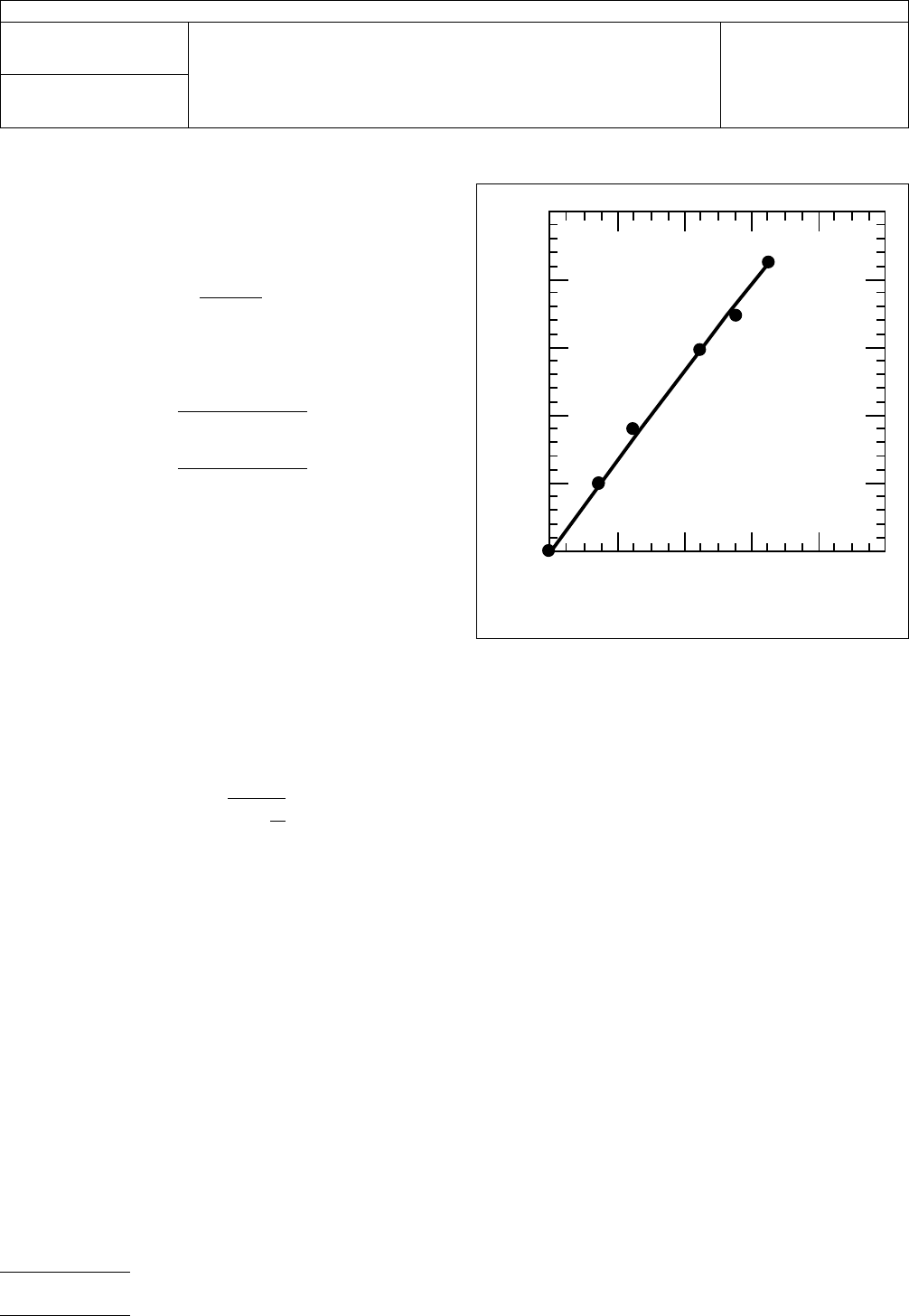
mation (y-axis) versus film thickness (x-axis). An equation of
theformy=mx(i.e. a straight line with intercept atx=0,y=
0) is fit to the data (unweighted) and the slope of the line can
be used to compare different materials or processes when
coated on identical substrates. A typical plot is illustrated in
Figure 1.
6.0 Notes
6.1
The
Flexus determines the radius of curvature by shining
a He-Ne laser beam through a beam splitter. The two beams
are reflected off the surface of the wafer into detectors. The
radius of curvature, R, is calculated from the angle of reflec-
tion and the distance between the two beams. If measure-
ments are made on the coated side of the wafer, the laser
beam is refracted twice, once upon entering the polymer layer
and again upon exiting the polymer layer. As the polymer layer
increases in thickness, the refracted laser beam can no longer
be correctly detected by the detector, resulting in erroneous
values for the radius of curvature. In practice, the upper limit
on thickness for polyimides was found to be approximately
10-12 µm. To avoid this complication, the polymer films are
deposited on the back of the wafers and the measurements
are made on the front (polished side) of the wafer. This
extends the useful thickness range to 50 µm.
6.2
The
radius of curvature will depend on the thickness of
the wafer. Wafers of comparable thickness (625 ± 15 µm)
must be used when making comparisons of different
materials.
2.4.22.2−01
Figure
1
Film Thickness (µm)
Curvature
Slope = 3.3
Wafer Deformation (
µ
m)
50
40
30
20
10
0
048
121620
IPC-TM-650
Number
2.4.22.2
Subject
Substrate
Curvature: Silicon Wafers with Deposited Dielectrics
Date
7/95
Revision
P
age2of2
电子技术应用 www.ChinaAET.com