IPC-TM-650 EN 2022 试验方法.pdf - 第353页
J-003061 Figure 2 Slump test stencil, IPC-A-20 ▼ Spacing ▼ 0.06 mm ▼ 0.10 mm ▼ 0.15 mm ▼ 0.20 mm ▼ 0.25 mm ▼ 0.30 mm ▼ 0.35 mm ▼ 0.40 mm ▼ 0.45 mm ▼ 0.40 mm ▼ 0.35 mm ▼ 0.30 mm ▼ 0.25 mm ▼ 0.20 mm ▼ 0.15 mm ▼ 0.10 mm ▼ 0…
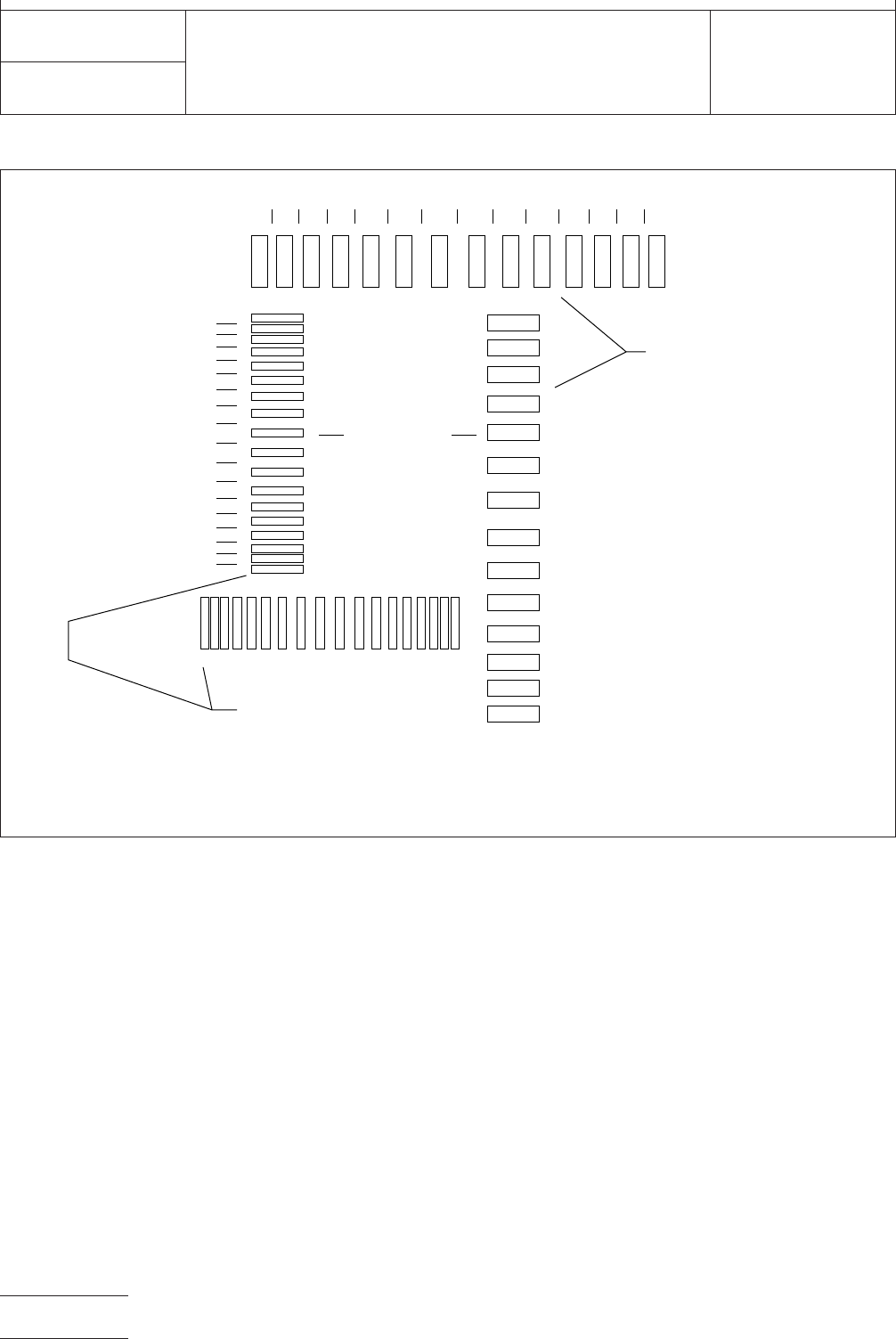
J-003060
Figure
1 Slump test stencil, IPC-A-21
▼
Spacing
▼
0.06 mm
▼
0.10 mm
▼
0.15 mm
▼
0.20 mm
▼
0.25 mm
▼
0.30 mm
▼
0.35 mm
▼
0.40 mm
▼
0.45 mm
▼
0.40 mm
▼
0.35 mm
▼
0.30 mm
▼
0.25 mm
▼
0.20 mm
▼
0.15 mm
▼
0.10 mm
▼
0.06 mm
Spacing
Vertical
Rows
▼
▼
▼
Pad Size:
0.33 x 2.03
mm
—18 identical pads per row
—Same spacings each row
▼
▼
Pad Size:
0.63 x 2.03
mm
—14 identical pads per row
—Same spacings each row
Spacing Spacing
▼
33mm
▼
.41
▼
.48
▼
.56
▼
.63
▼
.71
▼
.79
▼
.71
▼
.63
▼
.56
▼
.48
▼
.41
▼
.33mm
IPC-TM-650
Number
2.4.35
Subject
Solder
Paste—Slump Test
Date
1/95
Revision
P
age2of3
电子技术应用 www.ChinaAET.com
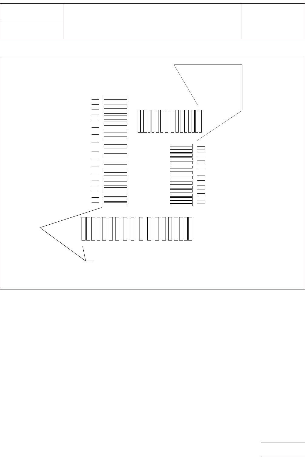
J-003061
Figure
2 Slump test stencil, IPC-A-20
▼
Spacing
▼
0.06 mm
▼
0.10 mm
▼
0.15 mm
▼
0.20 mm
▼
0.25 mm
▼
0.30 mm
▼
0.35 mm
▼
0.40 mm
▼
0.45 mm
▼
0.40 mm
▼
0.35 mm
▼
0.30 mm
▼
0.25 mm
▼
0.20 mm
▼
0.15 mm
▼
0.10 mm
▼
0.06 mm
Spacing
Vertical
Rows
▼
▼
▼
Pad Size:
0.33 x 2.03
mm
—18 identical pads per row
—Same spacings each row
Spacing
Spacing
Pad Size: 0.20 x 2.03
mm
—16 identical pads per row
—Same spacings each row
▼
▼
▼▼▼▼▼▼▼▼▼▼▼▼▼▼▼
0.075 mm
0.10 mm
0.125 mm
0.15 mm
0.175 mm
0.20 mm
0.25 mm
0.30 mm
0.25 mm
0.20 mm
0.175 mm
0.15 mm
0.125 mm
0.10 mm
0.075 mm
IPC-TM-650
Number
2.4.35
Subject
Solder
Paste—Slump Test
Date
1/95
Revision
P
age3of3
电子技术应用 www.ChinaAET.com

1
Scope
This
test method is used to simulate the proce-
dures for plated-through hole (PTH) component removal and
replacement, in order to determine the effects of rework on
the quality and integrity of the PTH barrel and conductor foil
on bare rigid or flexible printed boards. The five steps are
designed to simulate initial soldering after a preconditioning
bake and two subsequent replacements.
2
Applicable Documents
IPC-TM-650
Test
Methods Manual
2.1.1 Microsectioning
2.1.1.2 Microsectioning - Semi or Automatic Technique
Microsection Equipment
J-STD-004
Requirements
for Soldering Fluxes
J-STD-006
Requirements
for Electronic Grade Solder Alloys
and Fluxed and Non-Fluxed Solid Solders for Electronic Sol-
dering Applications
Commercial
Item Description (CID) A-A-59551
Wire,
Elec-
trical, Copper (Uninsulated)
3
Test Specimen
3.1
The
standard test sample shall be as specified in the
governing specification or standard. In certain situations, it
may be necessary to perform this test on a production printed
board. In this case, a minimum of three PTHs shall be
selected. For military printed board(s), the selected holes shall
contain the maximum number of internal layer connections, so
that a complete quality evaluation can be made.
Note: This is a destructive test.
4
Equipment/Apparatus
4.1
A
soldering and/or desoldering iron with temperature
control accurate within ± 6 °C [11 °F] of the preselected idle
temperature of 260 °C [500 °F], 315 °C [599 °F], or 371 °C
[700 °F] (see 6.2).
4.2
Tin
coated solid copper wire, conforming to (CID) A-A-
59551.
4.3
Liquid
soldering flux conforming to J-STD-004, Flux
Designator ROL1.
4.4
Rosin
fluxed solder Sn60Pb40A or Sn63Pb37A with
Flux Designator ROL1 (Rosin, Flux activity Type L1) conform-
ing to J-STD-006.
4.5 Metallographic
laboratory facilities, conforming with IPC-
TM-650, Methods 2.1.1 or 2.1.1.2.
4.6
Metallograph
capable of up to 200X magnification.
4.7
Forced
air convection oven capable of maintaining
121 °C to 149 °C [250 °F to 300 °F].
4.8
Shear
type wire cutters.
4.9
System
for solder removal (desoldering braid or vacuum
assisted desoldering tool).
5
Procedure
5.1
Condition
specimens in a forced air convection oven at
121 °C to 149 °C [250 °F to 300 °F] for a minimum of six
hours to remove moisture. After conditioning, allow the speci-
mens to cool to room temperature.
5.2
To
aid in the addition or removal of solder, flux may be
applied to both sides of the test specimen.
5.3
The
hand soldering and desoldering operation of the
wire shall be performed as follows:
Step 1: Solder wire into PTH
Step 2: Remove (desolder) wire from PTH
Step 3: Resolder wire into PTH
Step 4: Remove (desolder) wire from PTH
Step 5: Resolder wire into PTH
During the desolder and solder steps, solder every other PTH
in the row and allow the specimen to cool to room tempera-
ture. Then solder the remaining PTHs.
5.4
During
the solder and desoldering steps, the soldering
and/or desoldering iron shall have a tip temperature as follows
(see 6.1):
Method A: 260 °C [500 °F] - Default method
Method B: 315 °C [599 °F]
Method C: 371 °C [700 °F]
2215
Sanders Road
Northbrook, IL 60062-6135
IPC-TM-650
TEST
METHODS MANUAL
Number
2.4.36
Subject
Rework
Simulation, Plated-Through Holes for
Leaded Components
Date
05/04
Revision
C
Originating Task Group
Rework Simulation Task Group, 7-11c
Material
in this Test Methods Manual was voluntarily established by Technical Committees of IPC. This material is advisory only
and its use or adaptation is entirely voluntary. IPC disclaims all liability of any kind as to the use, application, or adaptation of this
material. Users are also wholly responsible for protecting themselves against all claims or liabilities for patent infringement.
Equipment referenced is for the convenience of the user and does not imply endorsement by IPC.
P
age1of2
ASSOCIA
TION CONNECTING
ELECTRONICS INDUSTRIES
®
电子技术应用 www.ChinaAET.com