Operating Instructions_VF335_en.pdf - 第201页
6|Function description d) In the [SU 1] register, enable a checkbox. ð If a checkbox is enabled, the PCB is processed by soldering module 1. ü Entering the offset points and the rotation angle for each PCB: a) Enter th…
6|Function description
6.9.13 Working with multiple panels
If you process boards with multiple panels, you do not have to generate separate
data sets for each individual panel (PCB). In the [Panel] dialog, you can copy the
data sets for identical single panels by giving details regarding numbers and co-
ordinates for the individual panels and by saving them in the soldering program.
Entering panel number, coordinates and rotation angle
ü To enter coordinates for multiple panels:
a) Click on the
button in the bottom toolbar of the [Soldering program editor]
dialog.
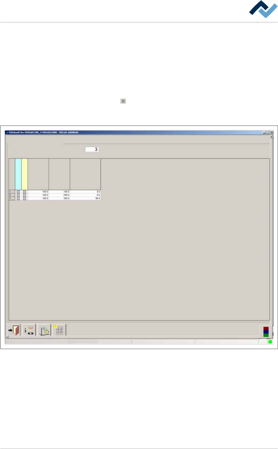
ð The [Panel] dialog is displayed:
Soldering program editor Panel data
Panel
No. of boards in panel
user: Service Maintenance mode
Offset X Offset Y Rotation angle
Board
Flux unit
Soldering unit 1
Fig.46: The [Panel] dialog
b) Enter the number of PCBs available in the panel in the input field [No. of
boards in panel].
ð The table below the input fields is then regenerated, depending on the
number of PCBs: A line is created for each individual PCB in the multiple
panel, in our example 3 PCBs. Previously displayed data is deleted during
this process.
ð The [Board] register shows the PCBs number.
c) In the [FM] register, enable a checkbox.
ð If a checkbox is enabled, the PCB is processed by the fluxer module.
Ersa GmbH Operating Instructions_VF335_en|Rev. 14|30/11/2017 200/695
6|Function description
d) In the [SU 1] register, enable a checkbox.
ð If a checkbox is enabled, the PCB is processed by soldering module 1.
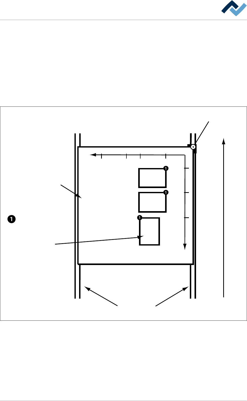
ü Entering the offset points and the rotation angle for each PCB:
a) Enter the offset X of the PCB in the [Offset X] register. The offset X is the dis-
tance in X direction from the barrier to point (1) of the PCB in mm.
b) Enter the PCB offset Y in the [Offset Y] register. The offset Y is the distance in Y
direction from the barrier to point (1) of the PCB in mm.
c) Enter the PCB rotation angle in the [Rotation angle] register. In our example, all
three PCBs are identical, although PCB 3 was rotated by 90°.
ð Please observe the following picture:
Single PCB
= Offset X/Y
Conveyor direction
Barrier (= Zero point)
Panel with three
PCBs
Conveyor
+Y
+X
350 200 100
100
200
300
180
2
3
1
Fig.47: Multiple panels:
There are three individual panels (PCBs) in this example; all of them are identical
except for single panel no. 3 which was rotated by 90° (mathematical positive dir-
ection of rotation, anti-clockwise).
Ersa GmbH Operating Instructions_VF335_en|Rev. 14|30/11/2017 201/695
6|Function description
6.9.14 Filing previous versions of soldering programs
In this dialog, you can influence the behavior by saving soldering programs.
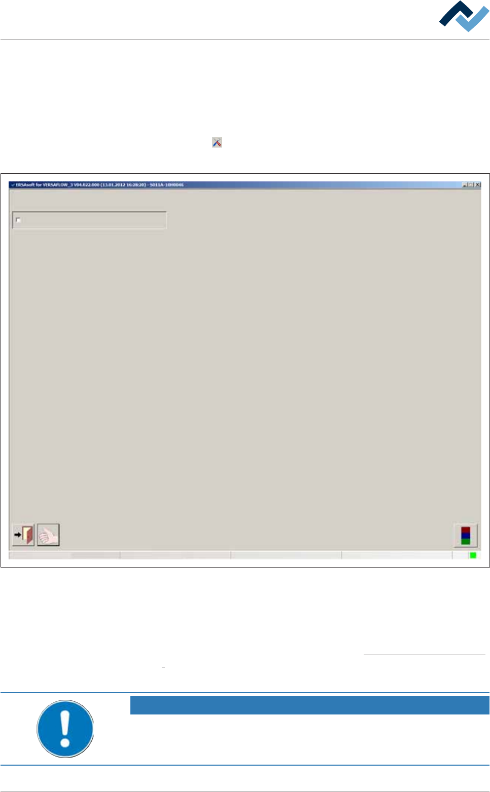
ü To archive the previous version of the soldering program:
a) Select first a library and then a soldering program in the [Soldering program ed-
itor] dialog.
b) Click on the
button in the bottom toolbar of the dialog.
ð The [Settings] dialog is opened:
Settings
User ersa
maintenance mode
Save History (unlimited)
Fig.48: The [Settings] dialog
c) Enable the [Save History (unlimited)] checkbox.
ð If you change and then save the soldering program, the previous version of the
soldering program is archived. The old soldering program is then automatically
filed in a new, subfolder. The new soldering program is saved in the current dir-
ectory path. On this regard , please read chapter The [File paths] editing dialog
[}139]. If you do not enable this checkbox, the soldering program is overwrit-
ten during each saving process. Previous versions are then no longer available.
NOTE
How can the content of an archived soldering program be displayed?
You can search for the archived soldering programs with Windows Explorer and show
them with an appropriate editor.
Ersa GmbH Operating Instructions_VF335_en|Rev. 14|30/11/2017 202/695