00195982-03_SM_SWS_EN.pdf - 第53页
3 SIPLACE wafer system (SWS) function 3.3 Pick and transfer process in detail Service Manual SIPLACE Wafer System (SWS) 11/2018 53 3.3 Pick and transfer process in detail 3.3.1 Flip chip segment 1 (nozzle) Fig.33: Flip …
3 SIPLACE wafer system (SWS) function
3.2 Basic die presentation process
52 Service Manual SIPLACE Wafer System (SWS) 11/2018
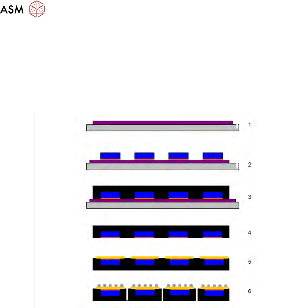
3.2.6 Embedded wafer level ballgrid array (eWLB/WLFO) process
Embedded wafer level ballgrid array is a packaging technology which makes it possible to produce
thin components with excellent electrical conduction with a 'chip fan out'. This means that the area
used for the connection pads is larger than the actual silicon, making sufficient space available for
the SMD process.
In this process, the chip components are placed with the active surface pointing downwards ("face
down") on a carrier with double-sided adhesive tape. After placement, this structure is molded.
After the die bond process of the carrier material, wafer structuring processes are used to create
the electrical contacts. In these, the molded area around the silicon is used as the carrier material
for "conductor tracks" ("fan out"). Finally, the components are tested, labeled and, for example,
packed in tapes.
Fig.32: Steps in the embedded wafer level ballgrid array process
1. The thermal release tape is laminated onto the metal carrier.
2. The active side of the wafer is placed face down onto the thermal release tape (flip chip)
3. Molding takes place under pressure, hardening at 150°C
4. Release
5. Redistribution layer (RDL)
6. Balling and single
7. Test, mark, pack
3 SIPLACE wafer system (SWS) function
3.3 Pick and transfer process in detail
Service Manual SIPLACE Wafer System (SWS) 11/2018 53
3.3 Pick and transfer process in detail
3.3.1 Flip chip segment 1 (nozzle)
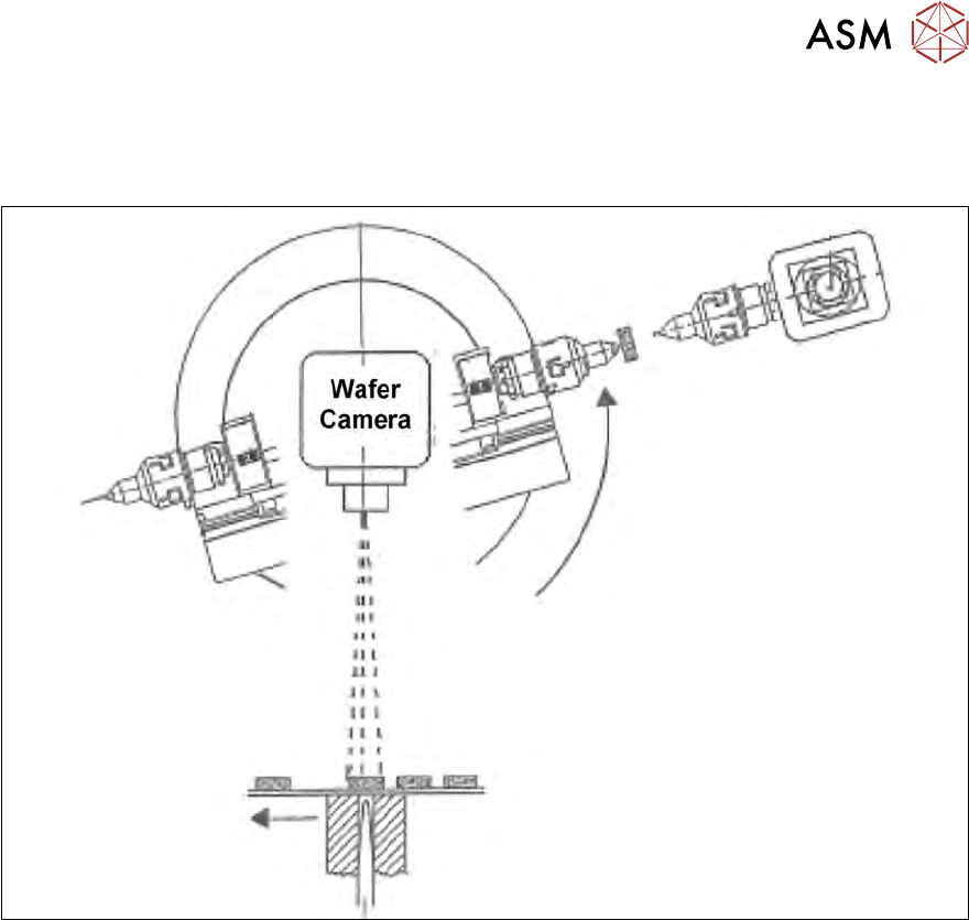
Fig.33: Flip chip segment 1 (nozzle)
●
The wafer X-Y travels to the next chip.
●
The flip chip rotary unit segment 1 turns to the handover position "Die Attach".
Image recognition of the next chip is performed from the camera "free" position.
3 SIPLACE wafer system (SWS) function
3.3 Pick and transfer process in detail
54 Service Manual SIPLACE Wafer System (SWS) 11/2018
3.3.2 Flip chip segment 1 (Z direction)
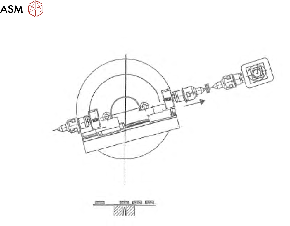
Fig.34: Flip chip segment 1 (Z direction)
●
The X axis of the flip chip rotary part, segment 1 is moved to the transfer position.