RS-1_instruction manual.pdf - 第1047页
Gl oss ary A − 1 Glossary − List of contai ned t erm s AT C Bad m ar k BGA, FBGA BOC ali gnm ent BOC m ar k Center i ng Com p onent data Com p onent shap e (“ C o mp Shap e”) Coor dinat e Cur r ent m em ory Data c om p a…

Appendix
Glossary ........................................................... A-1

Glossary
A−1
Glossary
− List of contained terms
ATC
Bad mark
BGA, FBGA
BOC alignment
BOC mark
Centering
Component data
Component shape (“Comp
Shape”)
Coordinate
Current memory
Data compatibility
Directory
EPU
Extension
Feed
Feeder (and similar units)
Feeder bank
Head (unit)
HMS
I/O safety direction setting
IC mark
IFS-NX
JaNets
Land
Lead
Machine coordinate origin
Mounter
MTC
MTS
Nozzle
OCC
Off-line
On-line
Origin return
Pick data
Picking
Pitch
Placement
Placement data
Placement station
PLCC
Program (production
program)
PWB data
PWB origin (coordinates of
the origin)
QFP
SOJ
SOP
Square chip
Support table
S-VCS
Teaching
Tray holder
VCS (unit)
Verify
Vision data
Glossary
A−2
ATC
An abbreviation for Auto Tool Changer
In RS-1/1R unit, nozzles that are suited to the component size are mounted on the head in
order to conduct component picking and placement. This is the storage place for these
nozzles.
Bad mark
A bad mark is as follows: On a gang processing PWB, a mark (bad mark) is affixed to a specific
part of the circuit that the user does not want to execute placement, the coordinates of the bad
mark are entered into Bad mark position of PWB data, and during production, the bad mark
reader moves to the coordinate position entered by the PWB data, and the OCC checks the
presence of bad mark, and as a result, the component will not be placed for a circuit that has a
bad mark
PWBs available for this system are gang processing PWBs. PWBs of single PWB processing
are not applicable. Use a bad mark with the diameter of 2.5 mm φ or larger, and the color
must be distinct in its light and shade.
Use of a white bad mark is preferable for a PWB of which color is relatively strong, such as
Glass Epoxy PWB while use of a blackish bad mark for a PWB of which color is light such as
ceramic PWB.
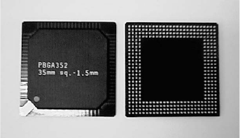
BGA, and FBGA
An abbreviation for Ball Grid Array, and Fine pitch BGA.
Solder bumps (balls) are arrayed in a grid pattern on the component placement surface. This
arrangement has a feature of having resistance against deformation and easiness of handling.
Since they were recently employed in Intel's peripheral circuits for personal computer, they are
adopted in the field of personal computer in a significant upsurge.
BOC alignment
This function recognizes the BOC mark and
calculates the correction rate by means of BOC
mark.
When to use BOC mark for placement, BOC
Alignment must be acquired. Otherwise,
placement position will be slipped when teaching of
placement position is conducted.
BOC mark
An abbreviation for Board Offset Correction mark.
A mark or marks provided on PWB to correct slippage between the periphery used in PWB
positioning or machine processing part such as positioning pin hole and the pad (land).
In RS-1/1R unit, two or three points of marks may be specified. Use of two points can correct
rotation and expansion/contraction. If three points are used, X and Y distortion can be
corrected in addition to the above.