RS-1_instruction manual.pdf - 第354页
Part 1 B asic O peration Chapter 4 Cr eating a Produc tion Progra m 4- 19 14) Global bad mark Enter the coor dinates of a position of a global ba d mark viewe d from the boar d refer ence position. When you s elect the &…
Part 1 Basic Operation Chapter 4 Creating a Production Program
4-18
9) Circuit pitch
Enter the distance between the circuits (the distance between the origins of two circuits, and
you have to enter a sign, + or – (minus).) in the X direction (or the PWB transport direction)
and in the Y direction (or the vertical direction to the PWB transport direction).
Example: data entry for a multi-plane matrix board
The circuit at the lower left corner is the reference circuit, and the lower left corner of the
circuit is the circuit origin in this example.
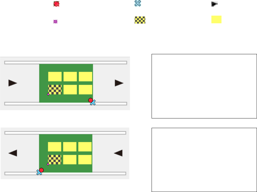
① For transport direction of L -> R
② For transport direction of R -> L
10) PWB height
11) PWB thickness
12) Back height
13) Clamp offset
Enter these menu items in the same manner as those for a single- circuit PWB.
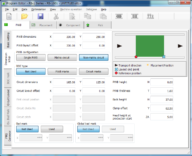
PWB dimensions X=200 Y=120
PWB layout offset X=5 Y=-5
Circuit dimensions X=50 Y=30
Circuit layout offset X=0 Y=0
First circuit position X=-170 Y=15
Circuit divide No X=3 Y=2
Circuit pitch X=60 Y=50
PWB dimensions X=200 Y=120
PWB layout offset X=-5 Y=-5
Circuit dimensions X=50 Y=30
Circuit layout offset X=0 Y=0
First circuit position X=-20 Y=15
Circuit divide No X=3 Y=2
Circuit pitch X=60 Y=50
:Board reference position :Layout end point :Transport
direction
:First circuit position :Reference circuit :Circuit
*Neither the first circuit position nor each circuit is displayed on the screen actually.
Part 1 Basic Operation Chapter 4 Creating a Production Program
4-19
14) Global bad mark
Enter the coordinates of a position of a global bad mark viewed from the board reference
position.
When you select the <Not Used> button, “***” is displayed in the “X” and “Y” coordinate input
fields.
15) Bad mark position
Select the <Not Used> button or the <Used> button depending on whether a bad mark is
used or not.
When you select the <Not Used> radio button, “***” appears in the “X” field and the “Y” field
respectively.
When you select the <Used> button, enter the distance from the circuit origin (circuit
reference position) to the center of a bad mark.
* In the above case, enter X = a and Y = b.
<Usage of a bad mark and operation flow>
i) Enter the bad mark coordinates into the PWB data.
ii) Before feeding a PWB, affix a bad mark on the spot specified with the bad mark
coordinates of a defective circuit.
iii) Before the start of production, the OCC reads a bad mark of each circuit. When a
bad mark is recognized, components are not placed on the corresponding circuit.
The requirements for a bad mark are: the mark must be distinct in the color
from a PWB, and its diameter must be 2.5 mm or greater. If a bad mark is
used, the production time will be longer by the mark recognition time.
* For the extended bad mark, refer to 4.3.3.5 "Extended bad mark."
* If the bad mark is set out of the circuit, use an extension bad mark.
a
Circuit origin (circuit reference position)
Bad mark coordinates
b
Part 1 Basic Operation Chapter 4 Creating a Production Program
4-20
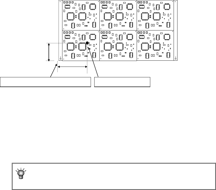
(4) Multi-plane non-matrix PWB
(set as “Non-matrix circuit” on the “Basic setting” screen)
The angle of each circuit is different from each other and the distance (pitch) between circuits is
not equal on this type of PWB.
Specify “X,” “Y” and “Angle” of each circuit on the “Circuit Layout” screen (see Section 4.3.3.4
“Circuit Layout”) to arrange circuits on a board.
Therefore, even though the pitch between two consecutive circuits is different from the other one
and/or the angle of one circuit is different from that of another one, the system can handle them
respectively.
If you specify the same circuit pitch and the same angle, you can create PWB data for a
multi-plane matrix PWB also.
1) PWB dimensions:
Enter the dimensions of the PWB including all circuits.
2) PWB layout offset:
Enter the length from the PWB position reference to the PWB layout end point in the same
way as a single-circuit PWB.
3) PWB configuration:
Select the <Non-matrix circuit> button.
4) BOC type:
◆ Not Used: Select this button when any BOC mark is not used.
◆ PWB marks: Select this button to use BOC marks on a board to correct the
component placement coordinates.
◆ Circuit marks: Select this button to recognize BOC marks of each circuit on a
multi-plane (circuit) board to correct component placement coordinates.
If there are many circuits on a board, this selection requires much time
to recognize marks, but the accuracy of component placement tends to
be higher than that when you select the <PWB marks> button.