RS-1_instruction manual.pdf - 第937页
Part 2 D etaile d Descript ion of E ach Functi on Chapter 12 Handling th e Optional Device s 12 - 53 12.10 Light for R ecognizing Solder If there is not any BOC m ark on a board or a circuit, t he system can ma ke the pr…
Part 2 Detailed Description of Each Function Chapter 12 Handling the Optional Devices
12-52
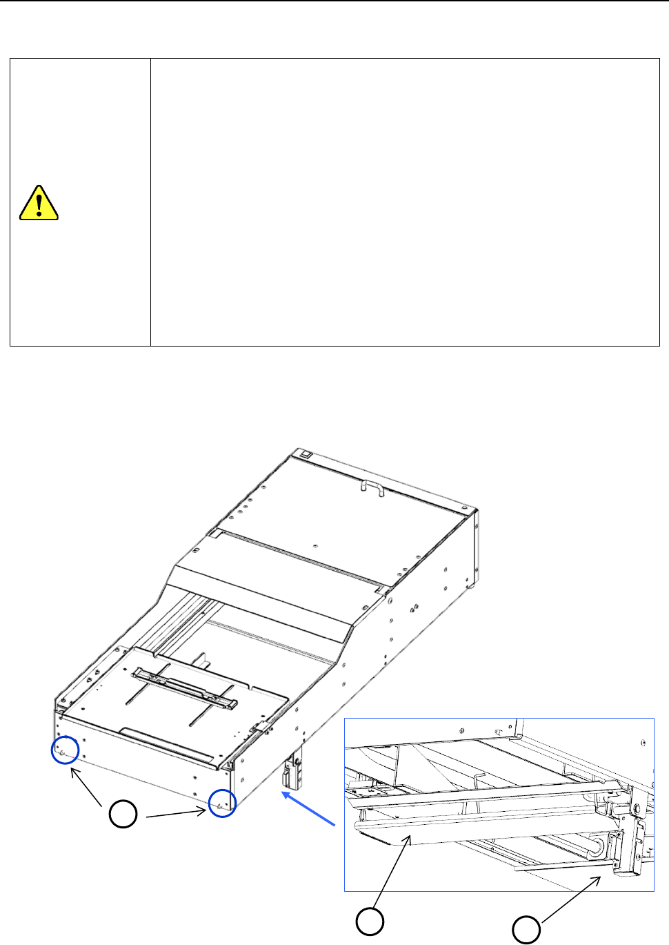
12.9 Dual Tray Server (DTS)
You can select a TR1RB as a DTS to be used with this machine.
Refer to the “INSTRUCTION MANUAL” of the DTS for how to handle it in details.
CAUITON
Do not replace the DTS with another one while the X- or Y-axis, or head is
operating. It may cause a serious injury to the operator or damage the machine
itself since the tray holder touches the operating parts.
Do not replace the tray holder with another one while the X- or Y-axis or head is
operating.
Be sure to open the safety cover before replacing a tray holder with another one.
After setting feeders required for PWB production at the positions specified with a
production program respectively, set feeders not to be used for production such
as an 8-mm tape feeder at all the positions not occupied with the feeders above
so that any finger or hand cannot be put between the set feeders to secure your
safety.
When using a tray with a thickness exceeding 10 mm, leave the rear feeder
floating sensor non-used. And you can use it by removing the regulation bar.
RS-1 operates with component height 25 mm only.
When using a tray with a thickness of 10 mm or less, use the rear feeder floating
sensor. If you install the regulation bar, it works according to the part height.
1) Attach the DTS at the desired position of the rear bank set with the “Machine Setup” screen.
Insert the positioning pin ① at the edge of the DTS into the bank.
2) Lock the clamp lever ② to fix the DTS.
3) Lower the I/F connector bracket ③ to insert the connector securely.
1
2
3
Part 2 Detailed Description of Each Function Chapter 12 Handling the Optional Devices
12-53
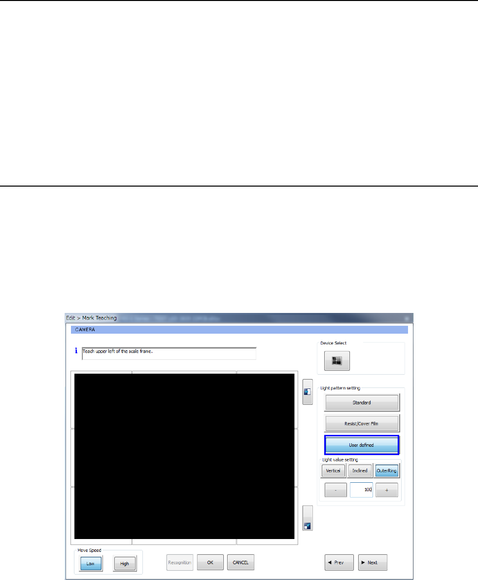
12.10 Light for Recognizing Solder
If there is not any BOC mark on a board or a circuit, the system can make the printed solder light
on to integrate it with a pad and recognize it as a BOC mark.
This function is to be used, for example, to place a component in an area in which a BOC mark
cannot be detected when a long-sized board is clamped twice.
If a soldered position is shifted from a pad largely, this function may not be able to be used.
If the “solder” shape is similar with that of a normal mark, which does not require any user template,
you can register it in the mark database and use it.
* Since the shape of printed solder is not clear as a mark, the component placement accuracy
may not become sufficient.
12.10.1 Teaching with using the light for recognizing solder
To improve the contrast between printed solder and a board, adjust each of the “Light value setting”
parameters: <Vertical>, <Inclined> and <OuterRing>.
<Procedure>
① Move the cursor to the mark position to be taught.
② Make the “Light pattern setting” before specifying the top left hand corner of the measurement
frame.
Select the <User defined> button and the <OuterRing> button, and then set the light value.
③ The procedure you shall follow after Step 2 above is the same as the normal procedure.
Part 2 Detailed Description of Each Function Chapter 12 Handling the Optional Devices
12-54
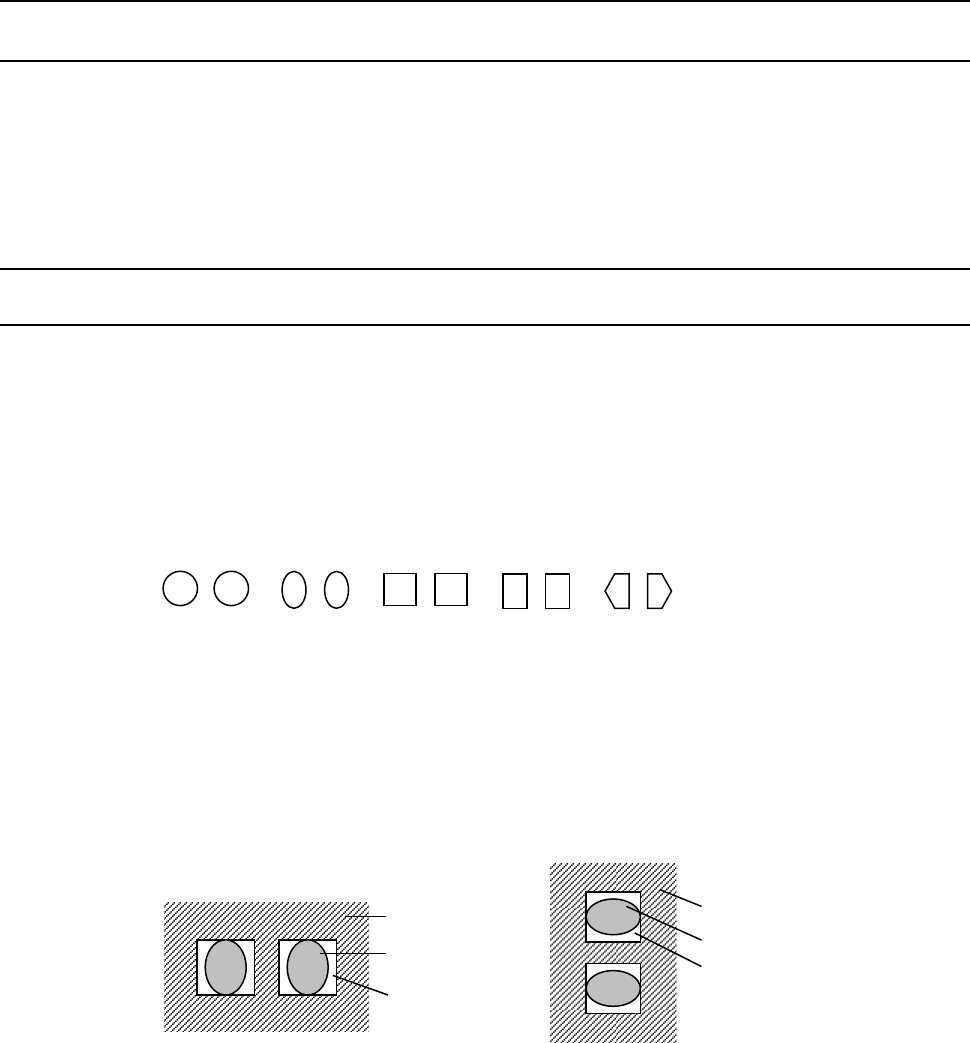
12.11 Offset Placement After Solder Screen-Printing
12.11.1 Functional Overview
There are two coordinate systems. One recognizes the BOC mark (pad) and the other recognizes
the solder. You can place components using either coordinate system on the basis of placing point.
When printing misalignment has occurred due to expansion/contraction of the PWB, the accuracy of
placing position after reflow can be improved by placing chip components, etc. on the solder and
using the self-alignment effect.
12.11.2 Specifications
12.11.2.1 Object to be recognized
① Applicable solder shape
A pair of cream solders, which are symmetrical, screen-printed on a PWB pad for a square
chip
* The shape of screen-printed solder should be symmetrical. The system cannot
accurately detect how much to correct the gap unless the shape is symmetrical.
The applicable shapes should be: circle, oval, square, rectangle and pentagon.
(* Recognition of other shapes should be checked.)
② Applicable chip size
0402, 0603, 1005, 1608, 2012, 3216
* Note that image of a set of solder whose shorter side is 0.16 mm or more and whose
longer side is 3.2 mm or less has to be obtained.
* Printing shall by stably conducted.
➂ Applicable solder angle
0°, 90°, 180°, 270° (Angle error for a camera: within ± 3°)
<Solder angle 0°,180°> <Solder angle 90°,270°>
④ Applicable board material and pad material
− Board material: glass epoxy, paper phenol, flexography, ceramic
− Pad material: gold, copper, hot air leveling
* The solder paste should have a certain level of contrast. If there is a portion whose
brightness is the same as that of solder in the area to be detected due to the condition
of the printed solder, serigraph, a pattern or PWB, and so any image that only solder
looks bright cannot be obtained, the system may not be able to correct the component
placement position by recognizing it. In such a case, you have to set the position of
solder paste again so that it can have the certain level of contrast.
PWB
Solder
Pad
PWB
Solder
Pad