RS-1_instruction manual.pdf - 第945页
Part 2 D etaile d Descript ion of E ach Functi on Chapter 12 Handling th e Optional Device s 12 - 61 12.11.7 Program Editor 12.11.7.1 Setting a Solder Mark Align the c ursor with the “ Mark Type ” c olumn of the area fid…
Part 2 Detailed Description of Each Function Chapter 12 Handling the Optional Devices
12-60
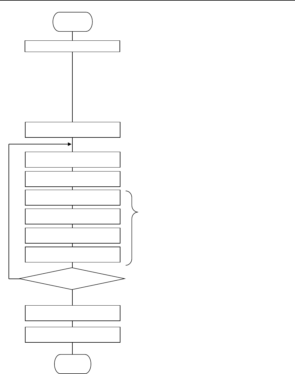
12.11.6 Flowchart for Setting a Solder Mark for Correction
① Select two or three points at which solder is to be
recognized among the component placement
coordinates specified in a production program.
* Select a position so that it can enclose the area in
which components are to be placed. If you select
three points, they should not be in the same
straight line.
* Any substance whose brightness is similar with
that of solder such as one printed in legend ink
should not be located near a position for
recognizing solder.
* It is recommended that a component placement
position to be recognized be on the bottom layer.
② Change the mark type of the area fiducial mark to
be used to recognize solder to “Solder.”
③ Enter the component placement coordinates
selected at Step ① as the mark coordinates.
④ Teach each mark.
⑤ If recognition is unstable even after using the
adjustment function, set another coordinate to
register a position that can be recognized stably.
⑥ Set the system to use an area fiducial mark to
correct a component placement point whose
solder misalignment is to be corrected.
Start
Teach a binary threshold value.
Enter the coordinates of a point to
be recognized.
Set the mark type to “Solder.”
Teach the lights.
Set the mark correction function for a
component placement point.
Teach the solder shape.
Set a misalignment check threshold
value.
Select a point to be recognized.
OK
NO
Register a mark.
Press the teaching button.
End
Recognition result?
Part 2 Detailed Description of Each Function Chapter 12 Handling the Optional Devices
12-61
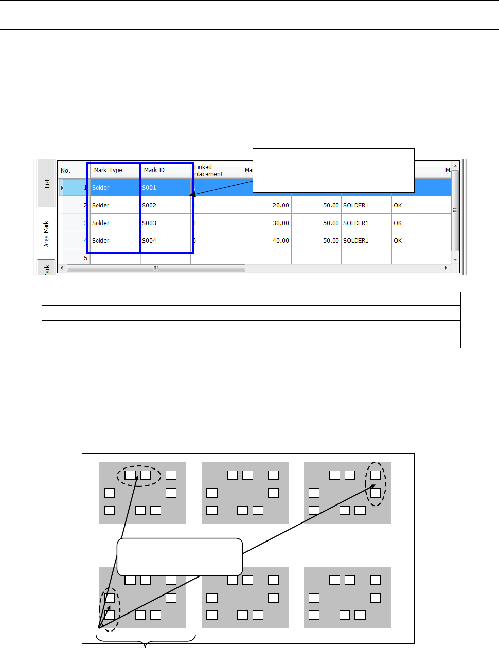
12.11.7 Program Editor
12.11.7.1 Setting a Solder Mark
Align the cursor with the “Mark Type” column of the area fiducial mark data, and click it with the right
button to select the mark type. You can specify up to 50 sets of area fiducial marks to be used for
recognizing screen-printed solder including normal marks. In addition, one set of solder
screen-printing positions can be registered at up to three positions. By default, a mark ID for
recognizing solder starts to be registered from [S001]. You can change this registered ID. When
you create a production program, you cannot register a solder recognition mark at a position on
which a component is already placed. Therefore, you have to set the solder mark layer to the last
layer.
Mark
Conventional area fiducial mark (default)
Solder
Solder mark per circuit
Solder (PWB)
Solder mark in the reference circuit coordinate system (for a multi-plane
board)
Select [Solder (PWB)] to recognize a pair of screen-printed solders on a multi-plane board to correct
misalignment. This selection enables you to register a coordinate outside the reference circuit,
and correct all circuits on a multi-plane board also based on the result of recognition of a pair of
screen-printed solders. Enter the recognized coordinates in the reference circuit coordinate
system. Note that you cannot set both [Solder] and [Solder (PWB)] as a mark type in one
production program.
When the system recognizes
screen-printed solder, “S” appears
before the mark ID by default.
Reference circuit
Enter the recognized
coordinates in the reference
circuit coordinate system.
Part 2 Detailed Description of Each Function Chapter 12 Handling the Optional Devices
12-62
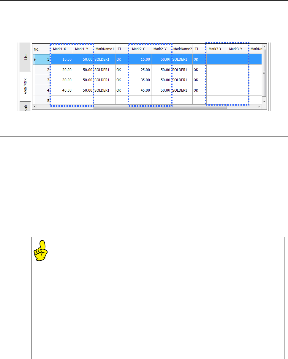
12.11.7.2 Entering a mark coordinate
Enter coordinates of two or three component placement positions to recognize solder in the “Mark X”
and “Mark Y” columns when you select [Solder] as the “Mark Type.”
However, when you select [Solder (PWB)] as the “Mark Type,” you can enter a coordinate value in
the reference circuit coordinate system even though it is outside the reference circuit.
12.11.7.3 Teaching
Adjust the cursor to the [TI] position and press the [Teaching] button in the operation area. Then,
execute solder teaching.
* The brightness of positions to be taught may vary because solder is used. Therefore, perform
not the Vision Copy function but the mark teaching operation.
(1) Light adjustment
While checking the VCS monitor, adjust each parameter: [Vertical Light], [Solder Light] and
[Contrast Pattern] so that the contrast between the screen-printed solder and a board can be
good.
Enter the desired value into the edit box directly or select the arrow mark located on the right
side of the edit box to change each parameter.
The setting of the [Vertical Light] mainly affects the brightness of a pad or resist section
of a board, and the setting of the [Solder Light] mainly affects the brightness of solder.
* When the system recognizes screen-printed solder, it converts the luminance of the
portion whose luminance is high such as an electrode pattern of a board to “0.”
Therefore, the system adjusts the parameters of the [Vertical Light] item and the
[Solder Light] item so that the luminance of the electrode pad section can look
highest, that of solder can look moderate, and that of other portions can look dark.
* If there are black spots (whose luminance is “0”) on the screen-printed solder due to
roughness of the surface of the screen-printed solder when the system adjusts a
binary threshold or recognizes the solder, set the luminance of the light so that it can
be darker than the set luminance.
* The setting of the [Contrast Pattern] item is a parameter that changes the sensitivity
of a camera. If the recognition condition cannot be improved by adjustment of the
lights, it allows the system to select the number that makes the contrast between the
screen-printed solder and the board good.