RS-1_instruction manual.pdf - 第363页
Part 1 B asic O peration Chapter 4 Cr eating a Produc tion Progra m 4- 28 Example: Data entry examp l e for a m ulti - pl ane non - matri x PWB On the assum ption that the lower left corner is t he PWB positi on refere n…
Part 1 Basic Operation Chapter 4 Creating a Production Program
4-27
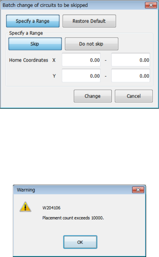
When you select the <Batch change of circuits to be skipped> button, you can specify circuits to
be skipped at a time by specifying the area of circuits to be skipped.
When you press the <Batch change of circuits to be skipped> button, the following screen
appears.
(1) Specify a Range
Specify whether to skip circuits whose origins are located in the area specified with the X
and Y coordinates set in the “Specify a Range” column.
(2) Restore Default
This button changes the skip settings of all circuits to the default settings.
When the total number of placement points exceeds 10,000 even though the number of
circuits is less than the regulated value, the following message appears on the screen.
Part 1 Basic Operation Chapter 4 Creating a Production Program
4-28
Example: Data entry example for a multi-plane non-matrix PWB
On the assumption that the lower left corner is the PWB position reference and the lower left
circuit is the reference circuit, an example of “circuit arrangement” is shown below.
* This varies depending on the transport direction and reference (front and rear).
The setting method is the same as that for "multi-plane matrix board."
Area check
When you input the data screen (for example, when you select the “Placement data”
screen), the system performs an area check, that is, it checks that the entered
coordinates of the BOC mark and those of the bad mark are on a PWB (or a circuit), or
all circuits are located within a PWB.
If the system detects an error, the following warning message appears on the screen.
• When you click the <OK> button, the system resumes switching the screen to the
selected one.
• When you click the <Cancel> button, the system stops switching the screen
* If the warning message shown above appears on the screen, review each value
entered on the PWB data.
(Check the settings of “PWB layout offset,” “First circuit position,” “Circuit layout
offset” and each coordinate entered on the “Circuit layout” screen especially.)
PWB dimensions X=330 Y=200
PWB layout offset* X=330 Y=0
Circuit dimension X=150 Y=100
Circuit. Layout offset X=0 Y=0
Circuit No.1 X=15 Y=0 θ=0
Circuit No.2 X=165 Y=100 θ=180
Circuit No.3 X=165 Y=0 θ=0
Circuit No.4 X=315 Y=100 θ=180
Circuit No.5 X=15 Y=100 θ=0
Circuit No.6 X=165 Y=200 θ=180
Circuit No.7 X=165 Y=100 θ=0
Circuit No.8 X=315 Y=200 θ=180
0°
180°
180°
180°
180°
Circuit
origin
Board reference position
0°
0°
0°
0°
120
100
30
15
Circuit 1 Circuit 2 Circuit 3 Circuit 4
Circuit 5 Circuit 6 Circuit 7 Circuit 8
Part 1 Basic Operation Chapter 4 Creating a Production Program
4-29
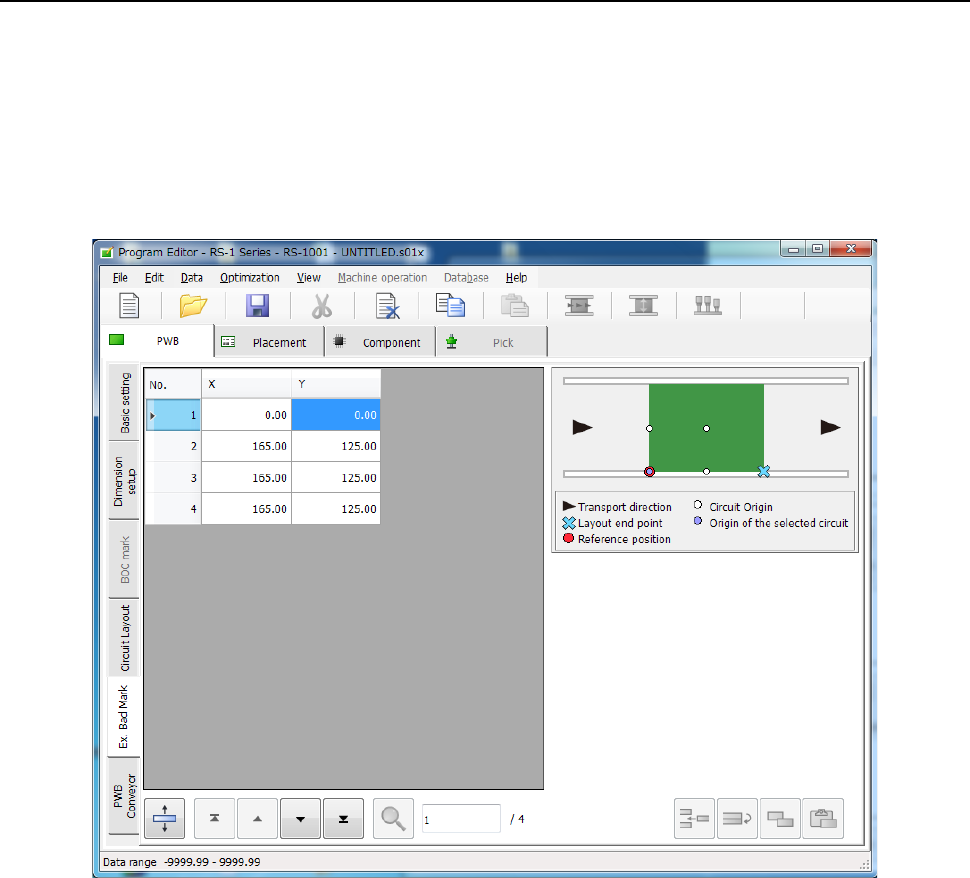
4.3.3.5 “Ex. Bad Mark” screen
For the extended bad mark, enter the "bad mark" position for each circuit from the "PWB reference
position."
Use this mark when the head moving distance for recognition is shortened or a mark cannot be
created in the circuit.
When you use an extended bad mark, enter the coordinates of a bad mark on each circuit.
When you select the “Ex. Bad Mark” tab displayed on the lower left of each “PWB” data screen,
the following screen appears.