RS-1_instruction manual.pdf - 第950页
Part 2 D etaile d Descript ion of E ach Functi on Chapter 12 Handling th e Optional Device s 12 - 66 ③ Manual adjustment From the [So lder Recogn ition Paramet er Setting] screen select [ Manual Adjustm ent] to manually …
Part 2 Detailed Description of Each Function Chapter 12 Handling the Optional Devices
12-65
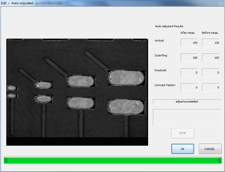
① (Parameter) Auto Adjust
When you select the <Auto Adjust> button on the “Set Solder Recognition Parameter” screen,
the system repeatedly changes each parameter to recognize a solder mark, and
automatically adjusts the parameters to the optimal ones. After the system automatically
finishes adjusting the parameters, the following “Auto-adjusted Results” screen appears.
If the system cannot recognize solder marks stably, it displays a warning.
When you press the F12 key on this screen, you can record two or more images displayed
during automatic adjustments. These images are stored in the same manner as the
recognized images displayed on the VCS monitor. However, this process requires much
time. To cancel this process, press the F12 key again or the Esc key. The dialog box
appears on the screen, and it allows you to cancel the image storage process or continue this
process.
② Recognized Result
When you press the <Recognized Result> button on the “Set Solder Recognition Parameter”
screen, the system recognizes solder marks according to the set parameters. When the
system succeeds in recognition, the cross mark appears at the center of the solder displayed
on the VCS monitor. If the system fails to recognize solder, the corresponding error code is
displayed on the VCS monitor. If the system cannot recognize solder stably, select the
<CANCEL> button on the “Set Solder Recognition Parameter” screen, and adjust the lights
again.
Part 2 Detailed Description of Each Function Chapter 12 Handling the Optional Devices
12-66
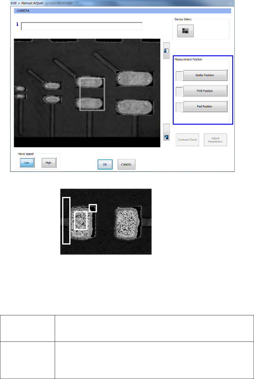
③ Manual adjustment
From the [Solder Recognition Parameter Setting] screen select [Manual Adjustment] to
manually adjust settings for solder, pads, resist and so on as well as adjustments to contrast
recognition and parameters.
- These images are stored in the same manner as the recognized images.
Teach each position: solder, PWB (especially wiring section) and pad in the “Measurement
Position” column. Align the cursor with the edit box corresponding to the position to be
taught, and use the HOD to teach it. When the system finishes teaching the position, *
(asterisk mark) appears in the corresponding edit box.
You may not be able to set the pad position. If so, proceed to the next step (using the
<Contrast Check> button and the <Adjust Parameters> button).
Contrast Check
The system measures the brightness of each area according to the parameters
currently set, and displays whether the obtained contrast is enough or not on the
screen.
Adjust Parameters
The system measures the brightness of each area while changing the recognition
parameters such as the light parameter to adjust the parameters so that enough
contrast can be obtained. The adjustment result is displayed on the
“Auto-adjusted Results” screen. If the system cannot obtain enough contrast
and cannot adjust the parameters, set the positions to be recognized again.
Part 2 Detailed Description of Each Function Chapter 12 Handling the Optional Devices
12-67
④ Detailed setting
Detailed setting for solder recognition can be made with the [Solder Recognition Parameter
Setting] screen.
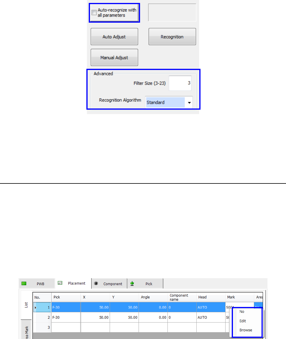
When you check the “Auto-recognize with all parameters” check box, the system changes all
of the parameters; lights, thresholds, and contrast pattern during automatic adjustment to
recognize solder with combinations of all patterns in order to adjust all parameters
automatically. Check this check box if the system cannot recognize solder stably even after
you select the <Auto Adjust> button on the “Set Solder Recognition Parameter” screen.
12.11.7.4 Setting the component placement position to be corrected
Select [Edit] or [Browse] in the menu displayed when you adjust the cursor to the [Mark] at the
placement point that requires solder print mis-alignment correction.
Select the [Edit] command or the [Browse] command on the displayed menu. Since the current
screen is switched to the area fiducial screen, align the cursor with the line of the solder mark that
has been taught and select it, and select the [Set] button. The mark ID to be used for correction
is displayed at the mark position of a component placement point whose misalignment correction
has been finished.
* When you want to set two or more component placement points to correct them at the same
time, align the cursor with the “Mark” column displayed on the “Placement” data screen and
drag all component placement points together to select them.