RS-1_instruction manual.pdf - 第942页
Part 2 D etaile d Descript ion of E ach Functi on Chapter 12 Handling th e Optional Device s 12 - 58 12.11.4 Operation option 12.11.4.1 Ig nore solder recognition error Selec t [Setting] – [Option sett ing] to open t he …
Part 2 Detailed Description of Each Function Chapter 12 Handling the Optional Devices
12-57
12.11.3.2.1 Setting an offset of the detection area
Set an offset value of the solder detection area with the “Set Margins for Detection Area” column
displayed on the “Solder Print Misalignment Correction” screen invoked from the “Function setting”
command of the “Setup” utility. Enter the desired value when you want to enlarge the detection
area based on the range calculated with the misalignment check value. The system recognizes
solder within the range obtained by adding the offset value to the misalignment check value.
* Even though you enter an offset value, the detection area is expanded only, and the judgment
value for the misalignment check does not change. However, when the detection area is
expanded, the system may by mistake detect solder not to be recognized, and recognition may
be unstable.
12.11.3.2.2 Setting the Initial Values for Teaching Solder
You can set the initial values of the parameters to be set for solder teaching.
You can set the following initial values for each mounter: [Solder Binary Threshold], [Misalignment
Check Threshold], [Area Check Threshold], [Vertical Light], [OuterRing] and [Contrast Pattern],
which are to be set for solder teaching.
When you select the <Default> button, all of the setting values are restored to the initial values set
at the factory.
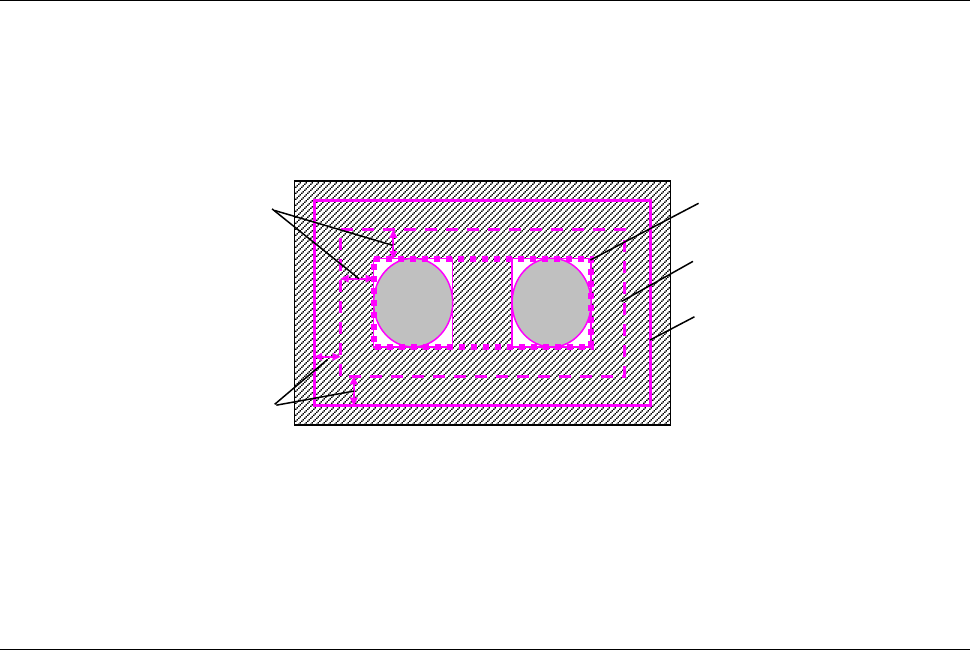
Detection area margins
Misalignment check values
Shape of solder
Default detection area
Detection area
Part 2 Detailed Description of Each Function Chapter 12 Handling the Optional Devices
12-58
12.11.4 Operation option
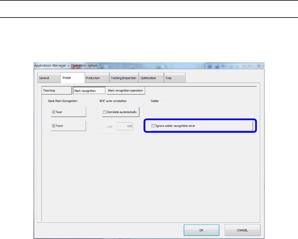
12.11.4.1 Ignore solder recognition error
Select [Setting] – [Option setting] to open the “Operation option” screen, and select the “Image”
tab and the “Mark recognition” tab. Check off or uncheck the “Ignore solder recognition error”
check box to specify whether to ignore a recognition error and place a component at the
placement coordinates.
If a solder mark recognition error occurs at even one position as a result of recognition of a set of
solder marks when the “Ignore solder recognition error” check box is enabled, the system places a
component at the normal position (without stopping temporarily) without correcting the placement
position related with the solder mark according to the solder mark.
* This “Ignore solder recognition error” function works during production only.
It does not work while a component placement position is being tracked with the camera as
specified with the Program Editor.
Part 2 Detailed Description of Each Function Chapter 12 Handling the Optional Devices
12-59
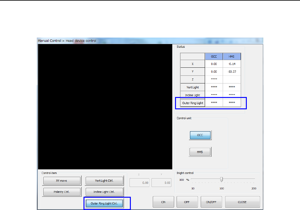
12.11.5 Manual Control
Select [Head] – [Head device control] in manual control to open the head device control dialog.
Then, select [Outer Device Control] of [Control item]. You can turn on and off each light by the
[ON], [OFF], and [ON/OFF] buttons.