RS-1_instruction manual.pdf - 第377页
Part 1 B asic O peration Chapter 4 Cr eating a Produc tion Progra m 4- 42 (10) Tr i a l Specify whether to per form a tr ial run or not. If you specify the comp onent placement po sition(s) with in the t rial - run ra ng…
Part 1 Basic Operation Chapter 4 Creating a Production Program
4-41
• Mark ID: Enter a mark ID. When you omit it, the system automatically assigns an
ID to the mark.
• Linked placement: Displays the number of placement data records that refer to the
area bad marks when you open the “Area Bad Mark” screen. You cannot
edit this item.
• X: Enter the X coordinate of the mark. The coordinate value can be obtained
with teaching operation.
• Y: Enter the Y coordinate of the mark. The coordinate value can be obtained
with teaching operation.
• Reference: Select the reference position of the coordinate system. Select “Circuit origin”
or “PWB origin.”
To change the setting, touch the input field to open the pop-up menu.
Select the desired reference position to enter it.
If you select any position on the pop-up menu when the cursor is located in
the “Reference” field and two or more lines are selected, the same value is
entered in all of the selected records.
PWB origin
Circuit origin
Set the coordinates viewed from the board origin.
Set the coordinates viewed from the circuit origin.
Note: You can select the [Circuit origin] command for a single-circuit board also. In this
case, set the coordinates viewed from the board origin.
When you open the pop-up menu with selecting the [Browse] command, any item described
above cannot be edited. When you open the menu with the [Browse] command, the screen
is displayed in Line Selection mode.
If you select any position on the pop-up menu when the cursor is located in the “Reference”
field and two or more lines are selected, the same position is entered in all of the selected
records.
• OK: Saves the edited data and returns to the “Placement” data list screen.
At that time, the use of mark group is not set.
• Cancel: Discards your editing and returns to the “Placement” data list screen.
When you double-click or press the Placement list tab to quit this “Area Bad Mark” screen,
the system redisplays the “Placement” data list screen without setting any link to the
Placement data.
The color of a bad mark should be able to be distinguished from that of a board, and
its diameter should be 2.5 mm or more. Note that when you use a bad mark, the
cycle time becomes longer by the mark recognition time.
(9) Skip
Specify whether to skip a component placement position displayed on this data screen.
“No” (a position is not skipped) is selected by default.
To change this setting, touch the input field to open the pop-up menu. Select the desired setting
to enter it.
If you select any item on the pop-up menu when the cursor is located in the “Skip” field and two or
more lines are selected, the same setting is entered in all of the selected records.
Yes
Skips the selected position.
No
Does not skip the selected position.
Part 1 Basic Operation Chapter 4 Creating a Production Program
4-42
(10) Trial
Specify whether to perform a trial run or not. If you specify the component placement position(s)
within the trial-run range on the production condition screen when setting the conditions for
trial-run, a trial run is conducted for only the placement data whose “Skip” item is set to “Yes.”
“No” (any trial-run is not conducted) is selected by default.
To change this setting, touch the input field to open the pop-up menu. Select the desired setting
to enter it.
If you select any setting on the pop-up menu when the cursor is located in the “Trial” field and two
or more lines are selected, the same setting is entered in all of the selected records.
Yes Conducts a trial run.
No Does not conduct a trial run.
(11) Layer
“Layer 4” is selected by default. To change the setting of this item, touch the input field to open
the pop-up menu. Select the desired layer to enter it.
If you select any layer on the pop-up menu when the cursor is located in the “Layer” field and two
or more lines are selected, the same layer is entered in all of the selected records.
When you execute the Optimization function, the component placement order is automatically
decided regardless of the input order.
The component placement order is optimized on the same layer. (If components run out during
PWB production, the system cannot proceed to production on the next layer until the system
finishes production on the layer whose number is smaller.)
Layer 1
Layer 2
Layer 3
Layer 4
Layer 5
Layer 6
Layer 7
First layer
Second layer
Third layer
Forth layer
Fifth layer
Sixth layer
Seventh layer
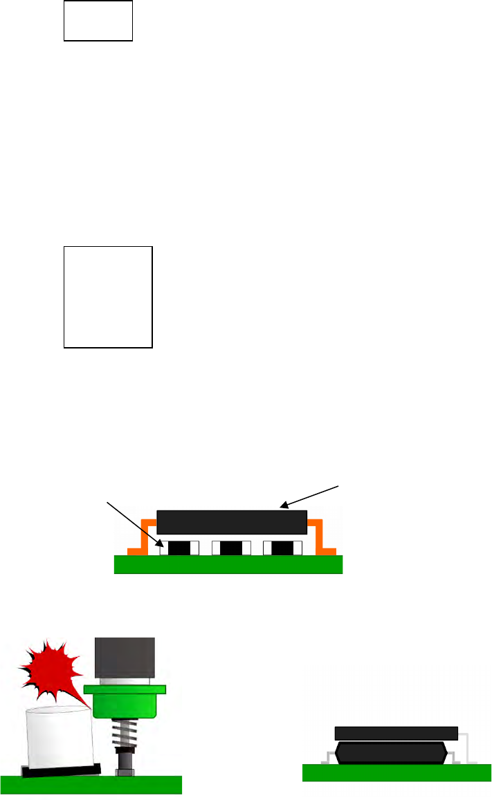
Example: If the system places QFP components and a chip component as shown in the right
figure, it has to place a chip component first.
In this example, when you specify the layer 4 for a chip component, and the layer 5
for a QFP, the system places a chip component whose layer number is smaller first,
and then a QFP.
<Placing QFP on the chip.>
・Layers are also used for adjacent placement/laminated placement.
<A component is placed near a tall one.> <IC components are stacked.>
Chip component (layer 4)
QFP(layer 5)
Part 1 Basic Operation Chapter 4 Creating a Production Program
4-43
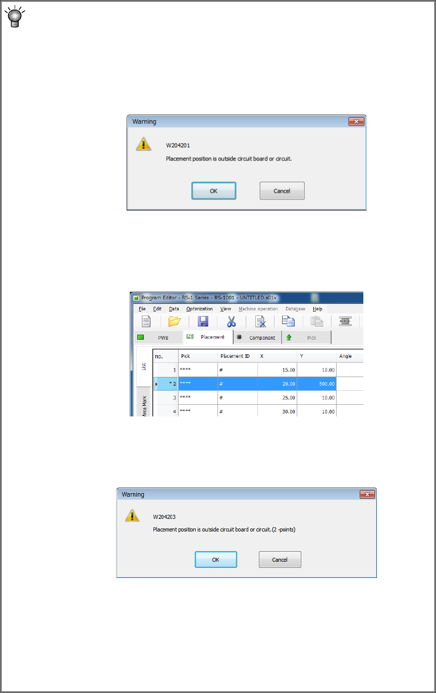
Area check
The system checks that a component placement position is within a PWB (for a
single-plane PWB) or within a circuit (for a multi-plane PWB) at the following timing:
1) At data entry
The system checks the component placement area when you enter or change
the placement coordinate X or Y.
If an error occurs, the system displays the following warning message.
• <OK>: The system validates data you entered, and displays an asterisk
mark (*) left to the placement data number indicating the range over
error (see the figure below). When you enter a value within the
range, this mark disappears.
• <Cancel>: The data you entered becomes invalid, and the system allows you
to enter data again.
2) When you switch the displayed data screen
When you switch the displayed data screen (for example, by selecting
component data), the system checks the component placement area.
If an error occurs, the system displays the following warning message.
• <OK>: The system resume switching the displayed data screen.
• <Cancel>: The system stops switching the displayed data screen.
* If the area check error occurs, check the data entered on the “Placement” data
screen. If you do not find any problem on this screen, check each entry on the
“PWB” data screen.
(Check the settings of “Reference hole position,” “PWB layout offset,” “First
circuit position,” “Circuit layout offset” and each coordinate entered on the “Circuit
layout” screen especially.)