RS-1_instruction manual.pdf - 第954页
Part 2 D etaile d Descript ion of E ach Functi on Chapter 12 Handling th e Optional Device s 12 - 70 12.12 Componen t Verificat io n (CVS) 12.12.1 Overv iew It checks the r esistanc e values, capacita nces and the polari…
Part 2 Detailed Description of Each Function Chapter 12 Handling the Optional Devices
12-69
12.11.8 Production
12.11.8.1 Processing an error at start of PWB production
When you try to use a mounter without this option and start PWB production with using the
screen-printed solder recognition function, the system displays the corresponding warning message
as a result of the check to be performed before PWB production starts.
When you try to start PWB production forcibly with pressing the START button, the dialog box
appears on the screen to state that the system cannot recognize any screen-printed solder.
Therefore, select whether to perform PWB production with ignoring recognition of the screen-printed
solder or cancel PWB production.
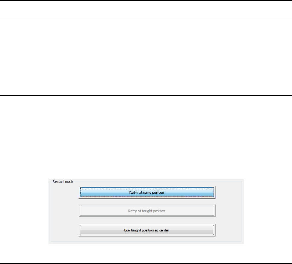
12.11.8.2 Error process during PWB production
You cannot select the menu item [Retry at taught position.], one of the production restart modes to
be displayed when a recognition error occurs. When you want to recognize solder without
changing the current position, select the menu item [Retry at same position.] and press the START
button. To perform teaching, select [OK] after teaching the middle point of a pair of solders, select
[Use taught position as center], and then press the [Production start] button.
To resume PWB production after releasing the clamp in the middle of PWB production, the system
cannot recognize solder at a position on which a component is already placed. Perform teaching
operation to set a solder screen-printing position again.
If a component is already placed on the solder mark position during continuous PWB production,
select the menu item [Use taught position as center.].
12.11.9 Operations with the Download production
To perform production online with enabling the “Offset Placement After Solder Screen-Printing”
check box, follow the instruction below.
• Specify a station in the Placement data so that a component placemen point used as a solder
mark can be on the last station in the line that can recognize solder. However, when you are
to optimize a production program with specifying the menu item [Fix all feeder positions within a
cluster] or the menu item [Alternate bank sides by program] of the “Multi-Optimize” option of the
Production Planning utility, a station you specified is ignored. Therefore, these Multi-Optimize
options cannot be used.
• When you use the Optimization function with the system software, you have to teach the solder
mark data with the main unit again.
• When a line is composed of two or more devices, a downstream device cannot register a solder
recognition mark at a position on which a component is already placed with an upper stream
device. If the Offset Placement After Solder Screen-Printing option is used in a line, it is
recommended that you set a different solder recognition mark with each device and that you
register a solder recognition mark at a position on which a component is placed with the last
downstream device.
Part 2 Detailed Description of Each Function Chapter 12 Handling the Optional Devices
12-70
12.12 Component Verification (CVS)
12.12.1 Overview
It checks the resistance values, capacitances and the polarities of the components fed at the start
of production and the restart of production after a shortage of component.
This is a function to check a wrong selection of reel. Up to 8 components can be checked
sequentially.
Note If a component pick-up position or supply direction is incorrect, this function may not
check a component correctly.
12.12.1.1 Applicable Components
This function checks the following components:
Applicable component type
Inspection conditions
- Square chip
- Laminated ceramic capacitor
- Tantalum chip capacitor
- Aluminum electrolytic capacitor
- Chip film capacitor
- 2-pin diode
- A component on whose bottom and opposite side two
electrodes are located
- A component whose interelectrode distance is 10 mm or less
- A component whose size is □ 10.00 mm or less
- Small component 0201 or larger
* Diodes are limited to general commutating diodes (other than light-emitting diodes and zener
diodes).
12.12.1.2 Items to Be Checked
This function checks the following items:
(1) Resistance
Measurable range: 10 Ω to 1 M Ω Measurement precision: ± 5% See Note 1
(2) Capacitance
Measurable range: 100 pF to 100 μF Measurement precision: ± 20 % See Note 1
(3) Diode polarity
Forward voltage: 1.8 V or less Open voltage range: 0 V to 4.3 V
Note 1: Measurement precision refers to a measurement error for a tolerance of a
component, and you have to specify the upper limit and the lower limit in the
Component data of a production program considering this precision.
Example:
For a square chip whose resistance error is ± 5 %, specify “10” as the upper limit,
and “- 10” as the lower limit.
12.12.1.3 Verification checking function
Two modes: “Continuous check mode” and “Single check mode” are provided, and functions
available in each mode are described below.
Part 2 Detailed Description of Each Function Chapter 12 Handling the Optional Devices
12-71
Tool menu
Operation mode
Description
Verify Current
check
Single check
Checks each component that caused an error in Continuous
verification mode.
Verify All check Continuous check
Checks all components or components that satisfy the requirements
you specified in a production program: checks up to 8 components
at the same time.
Single mode, the machine can check a component that failed to be
inspected.
* To use the verification function, a No. 7680 nozzle (for a 0201 or 03015 component) or the
following nozzle dedicated for the CVS is required.
Standard nozzles: 7500CVS, 7501CVS, 7502CVS, 7503CVS, 7504CVS, 7505CVS, 7509CVS
12.12.1.4 Actions to be taken during measurement
(1) Head used to pick up a component
8 axes can be measured simultaneously.
The system automatically selects a head that is used to pick up a component.
(2) Returning a component after checking it
The system returns some checked components onto their original positions, or discards other
ones depending on their packaging style as shown in Table below.
Since a component whose shorter side length is 1 mm or less may stand on its side or may be
turned over when it is returned, select the operation the system shall do on the dialog box.
- Components return and disposal conditions
Packaging
style
Requirement
When returning
a component
When discarding
a component
Tape
The shorter side is 1 mm or shorter.
Question dialog box *1
The shorter side is 1 mm or longer.
○
○
*2
*1 The system displays the dialog box to prompt you to select whether to return or discard a
component. When the system is set to measure components continuously, it displays
the dialog box at start of continuous measurement.
*2 The system discards a checked component when the menu item “Compo Reject to” is set
to “Trash conveyor” or “Protect.”
(3) Selection of a feeder from which the machine picks up a component
If the same type of components are assigned to two or more feeders (on the “Pick data”
screen), the machine starts picking up components in numerical order of holes form smallest
to largest by default. You can change this feeder order intentionally only in Single Check
mode.
(4) Changing the coordinates of a component pick-up position
When pick is not successful, perform teaching about coordinates and change the pick position
coordinates.