semi合集-English.pdf - 第1001页
SEMI E135-0704 © SEMI 2004 6 NOTE: These data are for conditions where the requested power went from 33% to 3% of the full power of the RF Generator being tested. Figure 3 Example of Digital Oscillosco pe Data that Shows…
SEMI E135-0704 © SEMI 2004 5
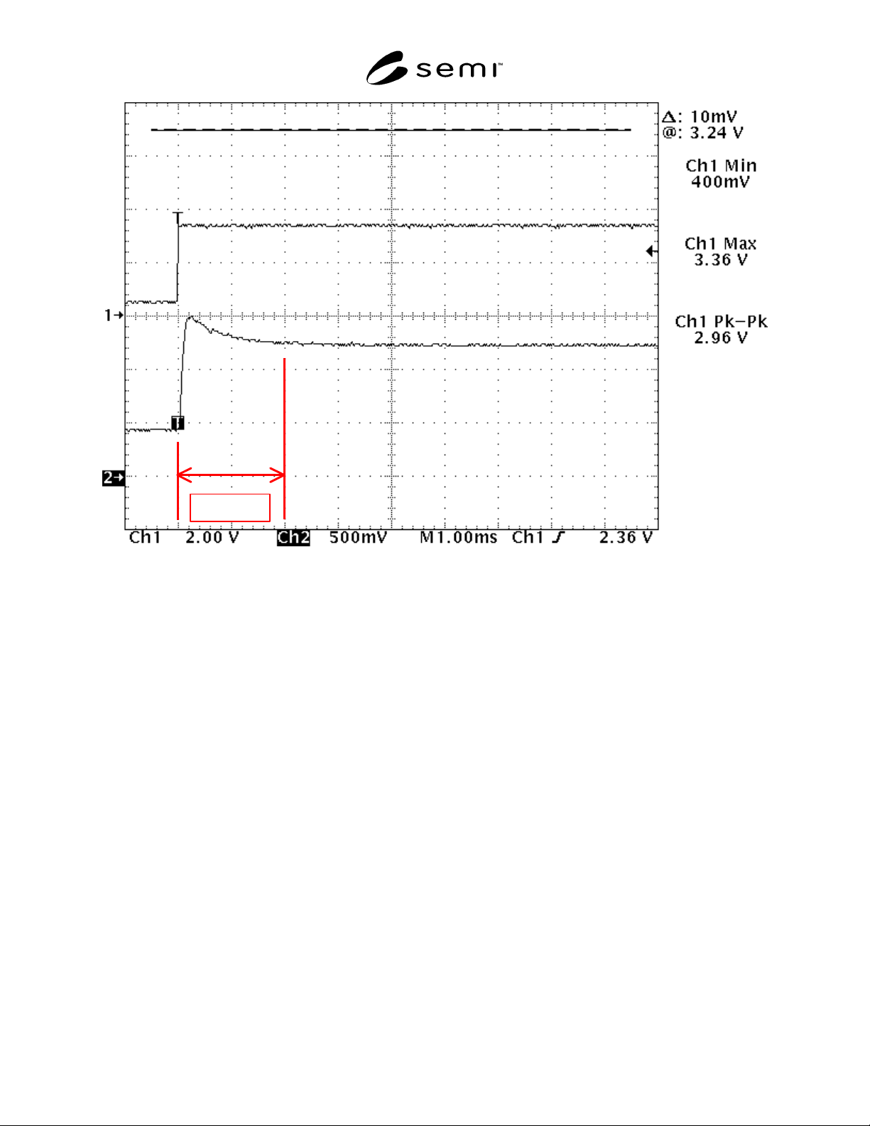
Transient
NOTE: These data are for conditions where the requested power went from 3% to 33% of the full power of the RF Generator
being tested.
Figure 2
Example of Digital Oscilloscope Data that Shows the Transient Response of the RF Output Power (Lower
Trace) Due to a Change in Set Point Signal (Upper Trace)
SEMI E135-0704 © SEMI 2004 6
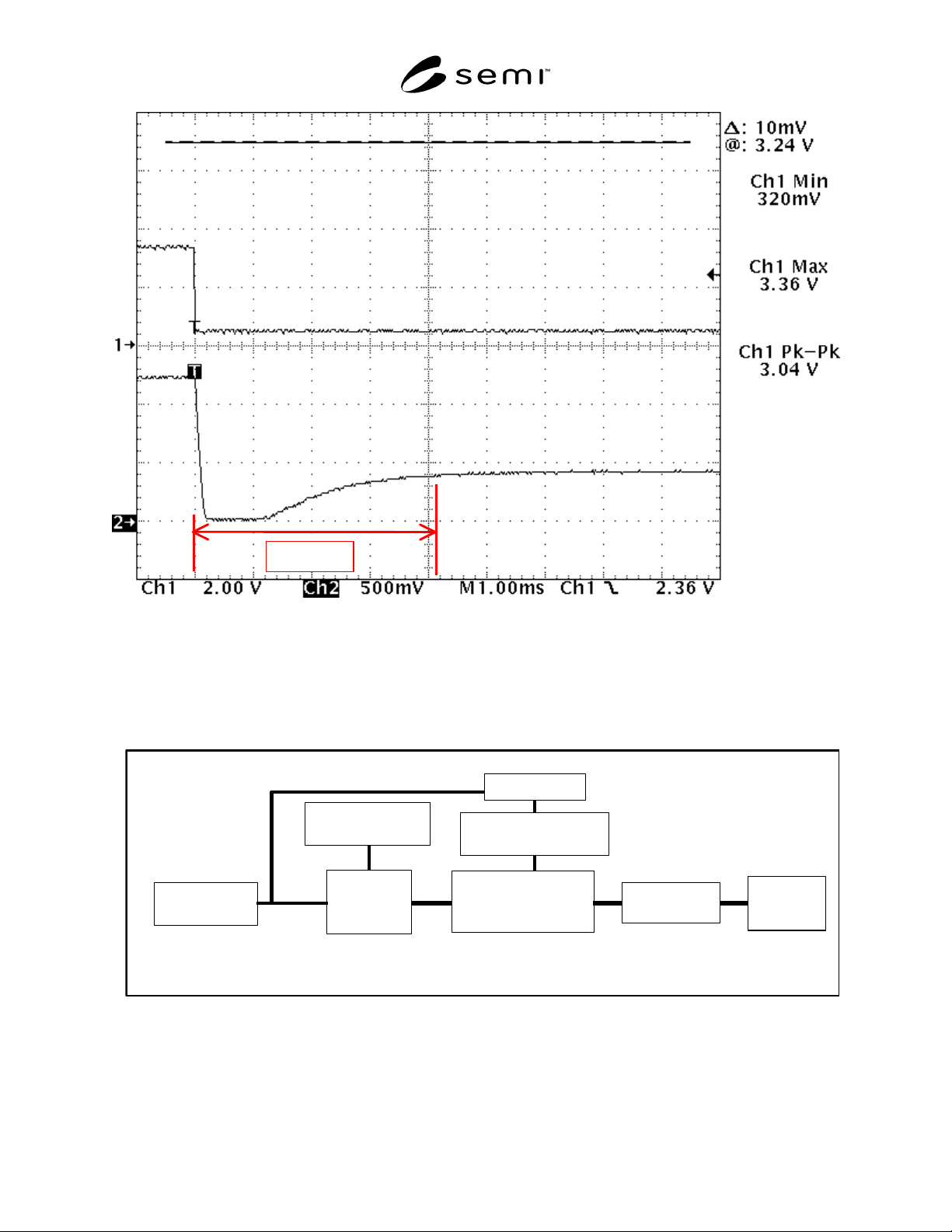
NOTE: These data are for conditions where the requested power went from 33% to 3% of the full power of the RF Generator
being tested.
Figure 3
Example of Digital Oscilloscope Data that Shows the Transient Response of the RF Output Power (Lower
Trace) Due to a Change in Set Point Signal (Upper Trace)
RF Signal Sample
r
D
irectional or
N
ondirectional
RF Powe
r
Mete
r
High-Power
RF Dummy
Load
R
F
Generator
(
DUT
)
RF Rectifier
/
Diode Detecto
r
Digital Scope
RF Enable
Signal Generato
r
RF Set-Point
/
Signal Generato
r
NOTE: If cable assemblies are used between the output of the RF Generator (DUT) and the High-Power Dummy Load, they shall
have the same nominal impedance as the DUT and shall have a power handling capability that is consistent with the maximum
output power of the RF Generator (DUT).
Figure 4
Schematic of the Test Setup for the Measuring the Transient Response of the RF Generator (DUT) as a
Function of a Change in the RF Enable Signal
SEMI E135-0704 © SEMI 2004 7
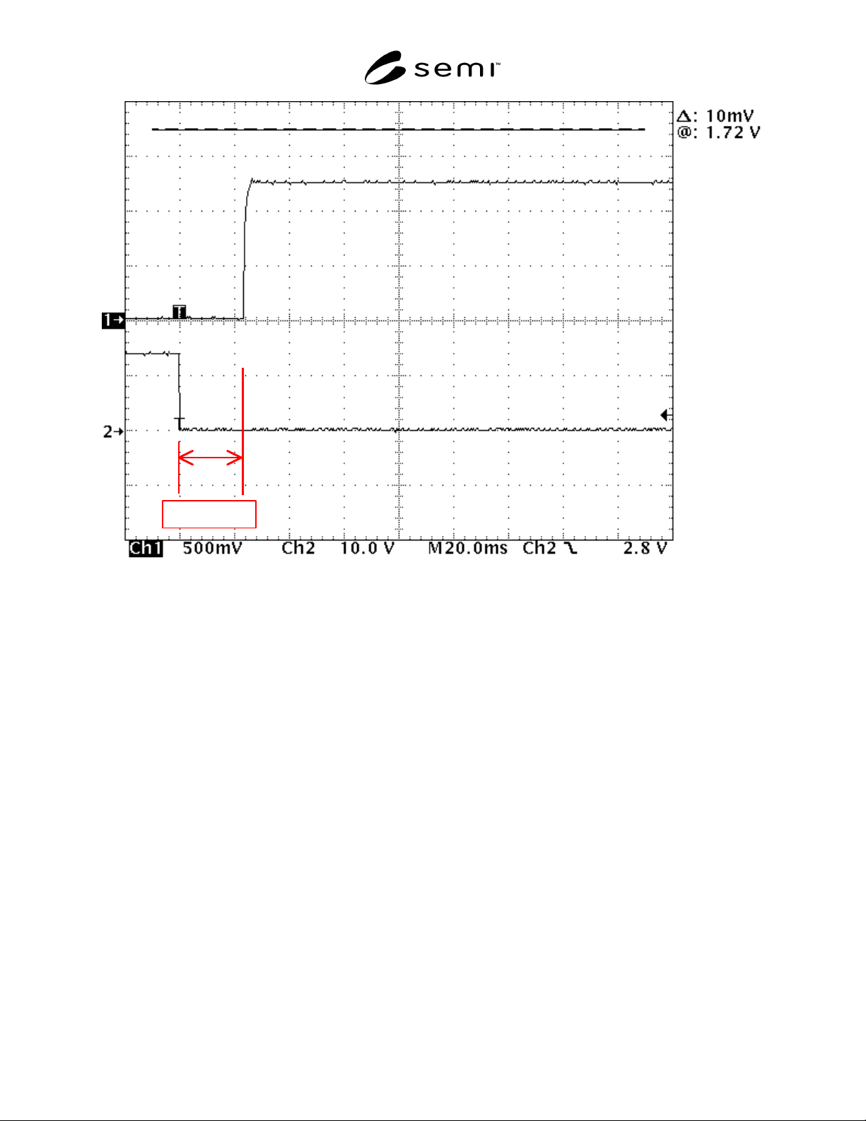
Time Delay
NOTE: These data are for conditions where the requested power went from 0% to 100% of the full power of the RF Generator
being tested.
Figure 5
Example of Digital Oscilloscope Data that Shows the Transient Response and Time Delay of the RF Output
Power (Upper Trace) Due to a Change in the RF Enable Signal (Lower Trace)
NOTICE: SEMI makes no warranties or representations as to the suitability of the standards set forth herein for any
particular application. The determination of the suitability of the standard is solely the responsibility of the user.
Users are cautioned to refer to manufacturer's instructions, product labels, product data sheets, and other relevant
literature, respecting any materials or equipment mentioned herein. These standards are subject to change without
notice.
By publication of this standard, Semiconductor Equipment and Materials International (SEMI) takes no position
respecting the validity of any patent rights or copyrights asserted in connection with any items mentioned in this
standard. Users of this standard are expressly advised that determination of any such patent rights or copyrights, and
the risk of infringement of such rights are entirely their own responsibility.
Copyright by SEMI® (Semiconductor Equipment and Materials
International), 3081 Zanker Road, San Jose, CA 95134. Reproduction o
f
the contents in whole or in part is forbidden without express written
consent of SEMI.