semi合集-English.pdf - 第995页
SEMI E131-0304 © SEMI 2004 5 RELATED INFORMATION 1 CALCULATION OF NOMINAL WAFER-SEATING PLANE NOTICE : This rela ted inform ation is not an official part of SEM I E131 and was derived f rom work by the originating task f…
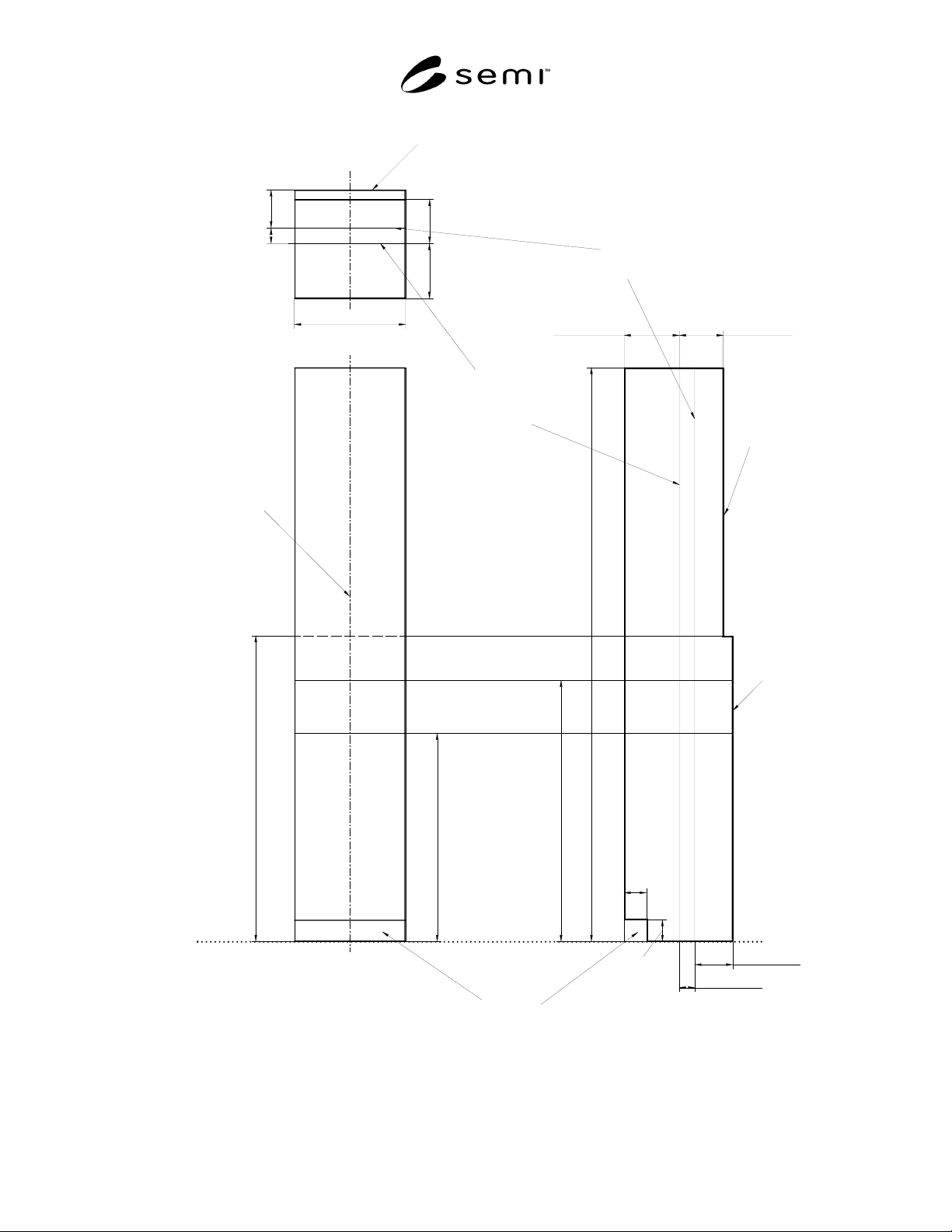
SEMI E131-0304 © SEMI 2004 4
plane
Equipment
Side ViewFront View
L (E64)
Top View
bilateral datum
floor
(E63)
(when carrier is undocked)
facial datum plane
(E63)
and removal)
substrate insertion
(when carrier is docked;
facial datum plane
BOLTS plane
(E63)
C
L
C
L
L
C
(E64)
Exclusion volume
(E64)
h
L
d
(E15.1)
boundary
(E63)
BOLTS plane
H2 (E15.1)
wafer-seating plane:
nominal
upper limit for
wafer-seating plane:
nominal
lower limit for
+(25-1)*z12 (E1.9)
+z8 (E1.9)
+z44 (E47.1)
H (E15.1)
+z8 (E1.9)
+z44 (E47.1)
H (E15.1)
+z79 (E63)
H (E15.1)
D (E15.1)
D1 (E15.1)
y76 (E63)
y70 (E63)
y70 (E63)
y76 (E63)
S (E15.1)
D (E15.1) D1 (E15.1)
Figure 1
IMM Dimensional Requirements

SEMI E131-0304 © SEMI 2004 5
RELATED INFORMATION 1
CALCULATION OF NOMINAL WAFER-SEATING PLANE
NOTICE: This related information is not an official part of SEMI E131 and was derived from work by the
originating task force. This related information was approved for publication by full letter ballot procedures on
December 4, 2003.
R1-1 The nominal wafer-seating plane is
calculated using values found in a number of
other standards, as follows.
R1-1.1 In SEMI E1.9 (the specification where this
plane is defined), the nominal wafer-seating plane is
referenced from the horizontal datum plane. SEMI
E15.1 defines the horizontal datum plane H to identify a
reference plane for positioning kinematic couplings.
While there are no kinematic couplings required for the
IMM, we use this same dimension as a starting point
for defining the nominal wafer-seating plane for wafer
insertion and removal. As in SEMI E15.1, the
horizontal datum plane is given at a height H relative to
the floor.
R1-1.2 Next, from SEMI E47.1 there is defined an
external horizontal datum plane (equal to the horizontal
datum plane from SEMI E15.1) and an internal
horizontal datum plane, where the internal horizontal
datum plane is located at a height of z44 above the
external horizontal datum plane.
R1-1.3 Then, FOUP slot number 1 is defined at a
height z8 in SEMI E1.9, but should be measured from
the internal horizontal datum plane from SEMI E47.1.
R1-1.4 Finally, z12 in SEMI E1.9 is the slot-to-slot
spacing within a cassette. So for a 25 substrate cassette,
the distance from the FOUP slot number 1 to slot 25 is
(25-1) * z12.
NOTICE: SEMI makes no warranties or
representations as to the suitability of the standards set
forth herein for any particular application. The
determination of the suitability of the standard is solely
the responsibility of the user. Users are cautioned to
refer to manufacturer' s instructions, product labels,
product data sheets, and other relevant literature,
respecting any materials or equipment mentioned
herein. These standards are subject to change without
notice.
By publication of this standard, Semiconductor
Equipment and Materials International (SEMI) takes no
position respecting the validity of any patent rights or
copyrights asserted in connection with any items
mentioned in this standard. Users of this standard are
expressly advised that determination of any such patent
rights or copyrights, and the risk of infringement of
such rights are entirely their own responsibility.
Copyright by SEMI® (Semiconductor Equipment and Materials
International), 3081 Zanker Road, San Jose, CA 95134. Reproduction o
f
the contents in whole or in part is forbidden without express written
consent of SEMI.

SEMI E135-0704 © SEMI 2004 1
SEMI E135-0704
TEST METHOD FOR RF GENERATORS TO DETERMINE TRANSIENT
RESPONSE FOR RF POWER DELIVERY SYSTEMS USED IN
SEMICONDUCTOR PROCESSING EQUIPMENT
This test method was technically approved by the Global Metrics Committee and is the direct responsibility
of the North American Metrics Committee. Current edition approved by the North American Regional
Standards Committee on April 22, 2004. Initially available at www.semi.org on June 2004; to be published
July 2004.
1 Purpose
1.1 The purpose of this document is to define a test
method used to determine the transient response for an
RF Generator used in RF power delivery systems for
semiconductor processing equipment to support SEMI
E113.
2 Scope
2.1 This document specifies the testing procedures and
test equipment required for determining the transient
response of an RF generator operating into a nominal
50-ohm load as a function of the change in set point
level, including the time delay between the request for
power (i.e., RF enable signal) and the start or stop of
the RF output signal.
2.2 The primary focus for this document is
semiconductor processing equipment including, but not
limited to, the following tool types:
• Dry etch equipment,
• Film deposition equipment (CVD and PVD).
NOTICE: This standard does not purport to address
safety issues, if any, associated with its use. It is the
responsibility of the users of this standard to establish
appropriate safety and health practices and determine
the applicability of regulatory or other limitations prior
to use.
3 Limitations
3.1 This standard addresses RF generators used in RF
systems that primarily operate in the frequency range of
0.2–100 MHz. It does not address higher frequency RF
systems or microwave systems.
3.2 This standard is meant for analyzing RF generators
that are designed to have a nominal characteristic
impedance of 50 ohms. This standard can also be used
with RF generators with a different characteristic
impedance if the appropriate standard terminations are
used.
3.3 International, national, and local codes, regulations
and laws should be consulted to ensure that the
equipment and procedures meet regulatory
requirements in each location.
3.4 This standard does not address any safety or
performance issues related to RF emissions or electrical
codes (e.g., Underwriter’s Laboratory, Inc. (UL), the
National Electrical Code (NEC), Federal
Communications Commission (FCC)). It is the
responsibility of the users of this standard to conform to
the appropriate local codes and regulations as applied to
this type of equipment, some of which are covered by
referenced documents.
4 Referenced Standard
4.1 SEMI Standard
SEMI E113 — Specification for Semiconductor
Processing Equipment RF Power Delivery Systems
NOTICE: Unless otherwise indicated, all documents
cited shall be the latest published versions.
5 Terminology
5.1 Abbreviations and Acronyms
5.1.1 CVD — Chemical Vapor Deposition
5.1.2 PVD — Physical Vapor Deposition
5.1.3 RF — Radio Frequency
5.1.4 VSWR — Voltage Standing Wave Ratio
5.2 Definitions of Terms
5.2.1 cable assembly — the section of cable
(transmission line), including the connectors, used to
connect various parts of the RF power delivery system.
5.2.2 device under test (DUT) — the RF generator to
be tested.
5.2.3 load impedance — the load impedance is the
impedance to which a generator is attached.
5.2.4 RF enable signal — the signal that a generator
receives to turn on the output power.
5.2.5 RF set point signal — the signal that a generator
receives that corresponds to a desired output power.