semi合集-English.pdf - 第974页
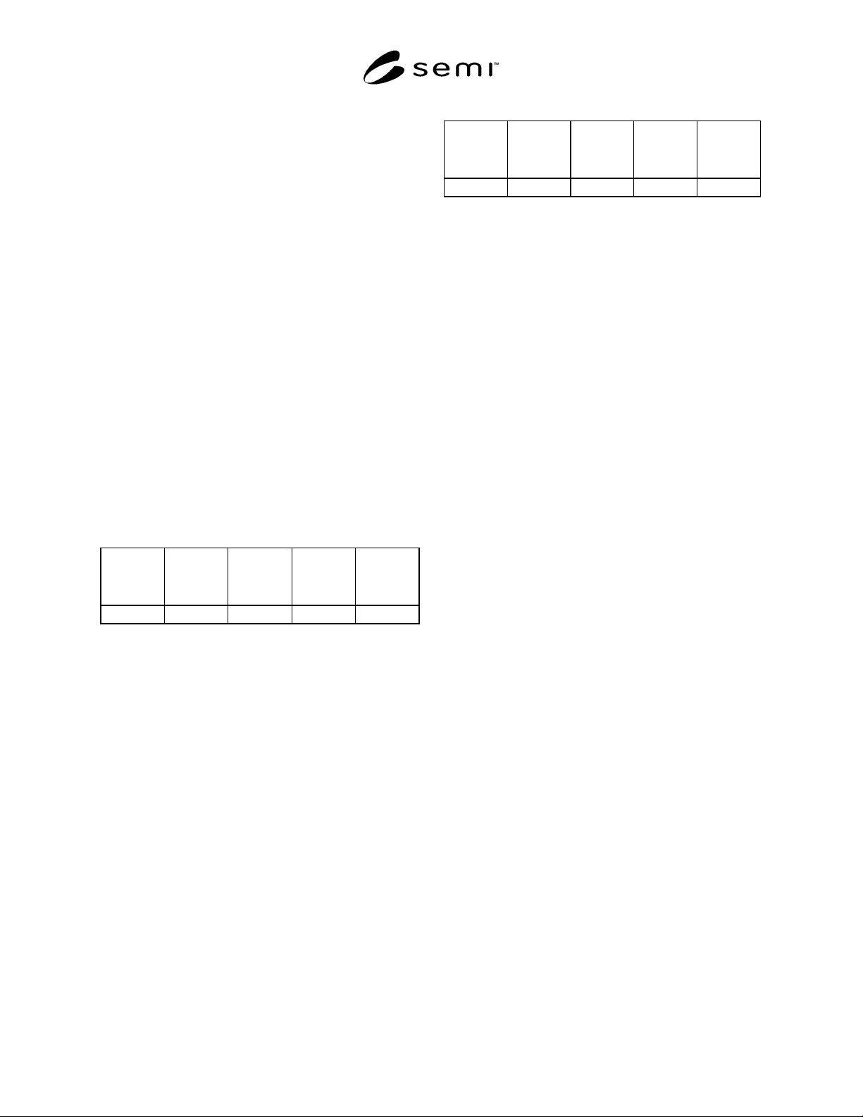
SEMI E129-1103 © SEMI 2003 12 Table A1-7 Elec trostatic Field Lev els – Limit Particle Deposition in a Class 1 Environment Year Node N/A, defects/cm 2 Electrostatic Field, V/cm 2000 180 nm 0.0141 180 2002 130 nm 0.0093 1…
SEMI E129-1103 © SEMI 2003 11
t = [N/A]/cv
elect
(2)
Using higher values of N/A in Equation 2 will increase
the acceptable values of t. Accepting higher values of c
will reduce max t.
A1-2.5.5 The value of the electrostatic field is initially
calculated at a distance of one wafer radius from the
wafer. While electrostatic field measurements can
certainly be made at this distance, they are typically
made at 2.5 cm (1 inch) with common instrumentation.
This is described in SEMI E43. Measurements made at
this smaller distance will be proportionally higher, but
under varying measurement conditions, it is difficult to
determine a precise relationship between electric field
and measurement distance. To provide a safety factor,
assume a linear relationship, rather than one
proportional to the square of the distance. For example,
with a 300-mm wafer, 3000 V/cm at 2.5 cm would
result in 500 V/cm at 15 cm.
A1-2.5.6 In SEMI E78, calculations were based on a
defect density N/A = 0.016 defects/cm
2
and a deposition
velocity v
elect
of 0.0105 cm/s. An example of the
resulting calculations is found in SEMI E78 Appendix 1
Table A1-2.2, a portion of which is shown in Table A1-
5.
Table A1-5 SEMI E78 Guide Table A1 – 2.2
E,
V/cm at
2.5 cm
N/A,
defects/
cm
2
v
elect
,
cm/s
ct,
s/cm
3
max t in
Class 1,
s
200 0.016 0.0105 1.524 1220
A1-2.5.7 Tables A1-6 and A1-7 below are derived
from Table A1-5 above, which is taken from SEMI E78
Appendix A1-2.2.2. They contain the same
assumptions used for the SEMI E78 table, but reflect
values for defect density (N/A) and particle deposition
velocity contained in the ITRS 2002 document for each
technology node. Assumptions are:
• Calculations are made for ISO Class 3 (formerly
Federal Standard 209E Class 1) where c ≤ 0.00124
particles/cm
3
.
• As contained in both the 1999 and 2002 ITRS,
particle deposition velocity is assumed to be 0.01
cm/s (2002 ITRS Yield Enhancement Chapter,
Notes Table 95a). Calculations are made assuming
the electrostatic deposition velocity, v
elect
, is equal
to this value.
• For N/A = 0.0141 defects/cm
2
as specified in the
1999 ITRS for the 180-nm node (Defect Reduction
Chapter, Table 77, assuming “Random Defects”
per mask layer are all the result of particle
deposition), the corresponding table becomes:
Table A1-6 Modified SEMI E78 Guide Table A1 – 2.2
E,
V/cm at
2.5 cm
N/A,
defects/
cm
2
v
elect
,
cm/s
ct,
s/cm
3
max t in
Class 1,
s
190 0.0141 0.01 1.41 1140
• The values from the 2002 ITRS (Yield
Enhancement Chapter, Table 91) N/A = 0.0093
defects/cm
2
as specified for the 130-nm node,
0.0089 defects/cm
2
for the 100-nm node, 0.0059
for the 65-nm node, 0.0056 for the 45-nm node,
0.0043 for the 32-nm node, and 0.0044 for the 22-
nm node technology are used.
• Calculations are normalized for an exposure time
of 1200 s (i.e., E values multiplied by 1140/1200).
• Relationship of electrostatic field, technology node,
and constant airborne particle concentration are
shown in Table A1-7.
• The years and technology nodes shown in Table
A1-7 correspond to those to be used in the 2003
ITRS.
A1-2.6 Recommendations for Induced ESD Damage
A1-2.6.1 The presence of electrostatic fields in
semiconductor manufacturing areas also creates the
potential for induced ESD damage. When an isolated
conductor is placed in an electric field, a charge
separation occurs in the conductor. If the conductor
momentarily touches ground, a flow of charge will
occur to the conductor. This flow of charge is a
potentially damaging ESD event. If the conductor, now
possessing excess charge, is removed from the electric
field, a second ESD event can occur when the
conductor contacts ground again.
A1-2.6.2 The most obvious example of these
phenomena occurs once the semiconductor device is
packaged. The package material is epoxy, an easily
charged insulator. The electric field from the charged
package induces a charge on the device leads. ESD
events occur when the leads contact ground during
processing.
SEMI E129-1103 © SEMI 2003 12
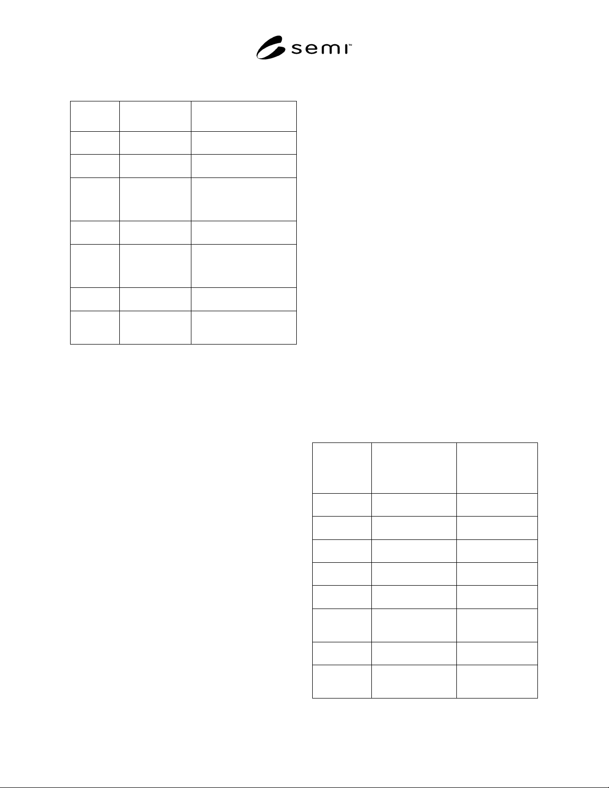
Table A1-7 Electrostatic Field Levels – Limit Particle
Deposition in a Class 1 Environment
Year
Node
N/A,
defects/cm
2
Electrostatic Field, V/cm
2000
180 nm
0.0141 180
2002
130 nm
0.0093 120
2003
100 nm
(2004)
(90 nm)
0.0089 114
2007
65 nm
0.0059 75
2009
50 nm
(2010)
(45 nm)
0.0056 71
2012
32 nm
0.0043 55
2015
25 nm
(22 nm)
0.0044 56
A1-2.6.3 A second problem for semiconductor
manufacturing occurs in the presence of a changing
electric field. This occurs when there is movement of
isolated conductors within an electric field, or the field
itself changes in magnitude. The result is that the
charge, and hence the voltage, induced on the
individual isolated conductors will not always be the
same, creating a potential difference between the
conductors. Under the right circumstances, ESD events
can occur between conductors at different potentials.
With the electric field changing, there is also the
likelihood that multiple ESD events will occur.
A1-2.6.4 This phenomenon of charge induced by
changing electric fields is mostly a concern in the
handling of photomasks with µm and sub-micron
feature sizes. While ESD damage occurred with 5×
photomasks with 3 to 5-µm features, it was infrequent.
At the 180-nm technology node, even 5× masks have
sub-micron features and the trend is to 4× masks,
making the feature sizes even smaller.
A1-2.6.5 The problem occurs because a photomask is
basically a large collection of closely spaced, isolated
conductors on an insulating quartz substrate. The
substrate is easily charged, creating an electric field.
The field changes whenever the spacing between the
photomask and ground changes (e.g., during handling
by robotics). Transporting the photomask, whether in
static dissipative reticle carriers or not, exposes it to
changing electric fields from other charged objects
(e.g., equipment panels, windows, work surfaces, and
equipment parts). The result is an increasing incidence
of ESD damaged photomasks as geometries shrink.
A1-2.6.6 While there have been several studies
documenting the existence of the field charging
problem on photomasks, there is currently a need for
further research to demonstrate the level at which it
occurs for production facilities. A recent study
(Montoya, et al.) was able to produce the following
information:
1. Testing was done on a photomask test device with
1.5-µm gaps between features. Approximately 800
V/cm (2 kV/inch) of electric field was needed to
cause damage.
2. Current production 180-nm photomasks are 4×
with a nominal gap width of 0.72 µm (or less
depending on the technology). ESD should occur
at 400 V/cm (1 kV/inch) or less.
3. To avoid ESD on 180-nm photomasks, electric
fields should be kept below 50% of the damage
threshold, or 200 V/cm (500 V/inch).
A1-2.6.7 Table A1-8 below is based on these
measurements. It is acknowledged that discharge
phenomena may change at very small conductor
spacing, and that the relationship to electric field may
not be a linear function of the geometry. The values in
Table A1-8 may need to be changed as more
information becomes available.
Table A1-8 Electrostatic Field Levels – Limit Induced
ESD Damage on Photomasks
Year
Node
Electrostatic Field
Limits
Induced ESD Damage,
V/cm
Electrostatic Field
Limits
Particle Attraction,
V/cm
2000
180 nm
200 (200) 180
2002
130 nm
144 (150) 120
2003
100 nm
111 (125) 114
2004
90 nm
100 (100) 114
2007
65 nm
72 (70) 75
2009
50 nm
(45 nm)
55 (50) 71
2012
32 nm
35 (35) 55
2015
25 nm
(22 nm)
27 (25) 56

SEMI E129-1103 © SEMI 2003 13
A1-2.7 Guide Recommendations
A1-2.7.1 This document recommends the values
shown in parentheses in the second column of Table
A1-8 of this Appendix and includes them in Section
12.5 Table 1.
A1-2.8 Guide Recommendations for Equipment
Malfunctions
A1-2.8.1 Most semiconductor manufacturing
equipment should comply with the ESD immunity
requirements of the European Economic Community
(EEC). The testing mandated by the EEC uses the test
methods and ESD immunity levels specified in IEC/TS
61000-4-2. To test for compliance, measurements are
made with an ESD simulator described by IEC/TS
61000-4-2. Equipment is required to pass a test
involving the discharge produced by a 150-pF capacitor
charged to 4000 V, or 600 nC.
A1-2.8.2 Users should note that the above test
discharge level and properties (i.e. discharge voltage,
discharge model and pulse rise time) may not be
sufficient to predict actual discharges that occur in
semiconductor production environments. In addition,
the ESD immunity of equipment in an isolated test
environment may change when it is installed in a
production environment.
A1-2.8.3 The discharge test specified in IEC/TS
61000-4-2 is done at significantly higher charge levels
than are recommended for objects in the facility in
Table A1-2 of this Appendix. If the recommendations
of Table A1-2 are followed, static charge levels should
be low enough to prevent ESD-induced equipment
malfunctions.
A1-2.8.4 If the recommended electrostatic levels
regarding ESD contained in Section 12.5 Table 1 are
not used, those contained in SEMI E78 should be used
for equipment.
A1-3 References
SEMI E78 — Electrostatic Compatibility
– Guide to
Assess and Control Electrostatic Discharge (ESD) and
Electrostatic Attraction (ESA) for Equipment
Montoya, J. A., Levit, L., and Englisch, A., “A Study of
the Mechanisms of ESD Damage for Reticles”,
Electrical Overstress/Electrostatic Discharge
Symposium Proceedings, 394-405 (2000)
Cooper, D. W., Miller, R. J., Wu, J. J., and Peters, M.
H., "Deposition of Submicron Aerosol Particles During
Integrated Circuit Manufacturing: Theory", Particulate
Sci. Technol. 8 (3 and 4): 209-224 (1990)
Liu, B. Y. H., and Ahn, K. H., "Particle Deposition on
Semiconductor Wafers", Aerosol Sci. Technol. 6: 215 -
224 (1987)
International Technology Roadmap for Semiconductors
(1999, 2002, 2003)
8
ISO 14644 – Cleanrooms and Associated Controlled
Environments – Part 1 – Classification of Air
Cleanliness
9
NOTICE: SEMI makes no warranties or
representations as to the suitability of the standards set
forth herein for any particular application. The
determination of the suitability of the standard is solely
the responsibility of the user. Users are cautioned to
refer to manufacturer’s instructions, product labels,
product data sheets, and other relevant literature
respecting any materials mentioned herein. These
standards are subject to change without notice.
The user’s attention is called to the possibility that
compliance with this standard may require use of
copyrighted material or of an invention covered by
patent rights. By publication of this standard, SEMI
takes no position respecting the validity of any patent
rights or copyrights asserted in connection with any
item mentioned in this standard. Users of this standard
are expressly advised that determination of any such
patent rights or copyrights, and the risk of infringement
of such rights, are entirely their own responsibility.
8 International SEMATECH, 2706 Montopolis Drive, Austin, TX
78741, USA (www.sematech.org)
9 Institute of Environmental Sciences and Technology (IEST), 5005
Newport Drive, Rolling Meadows, IL, 60008-38411, USA
(www.iest.org)