semi合集-English.pdf - 第5227页
SEMI M40-0200 © SE MI 2000 9 Table 2 Scan Pattern Locations Location X, Y Coord inates (per SEMI M20) Scan Dir ectio n (for line and ar ea tools), parallel to: Center P oint 0, 0 Y-axis 5-point Pattern Point # Loc ation …
SEMI M40-0200 © SEMI 2000 8
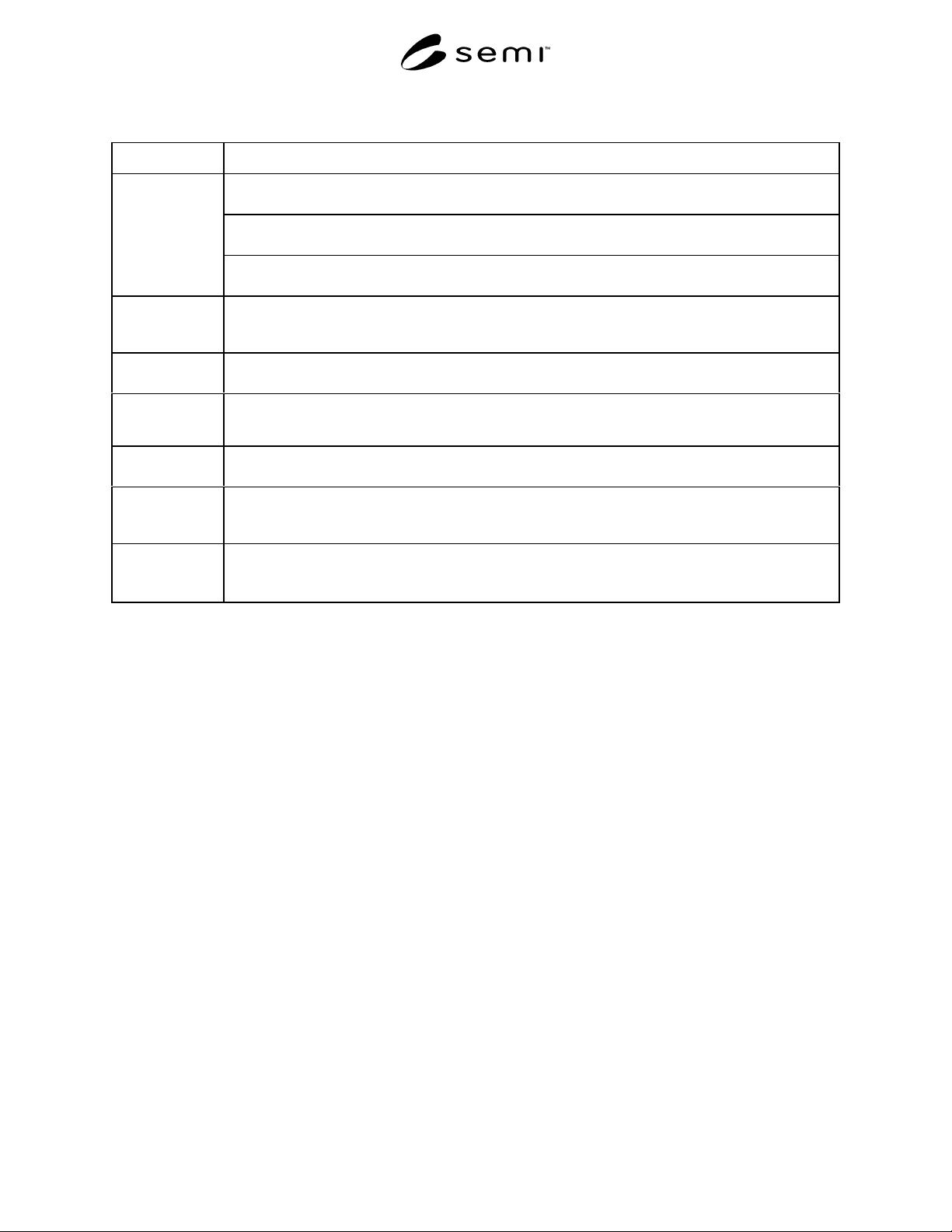
Table 1 Roughness Measurement Codes
Element Abbreviation Item
A12 3 4
Profilometer AFM SPM OPR MPR
B1
Interferometer IM
C12 3
Instrument
Scatterometer TIS ARLS SSIS
159 R C SPattern
(See NOTE 1.)
Center 5-point 9-point FQA/Raster
scan
FQA/Concentric
R-theta scan
FQA/Spiral
R-theta scan
ABPattern
Orientation
AB
PLALocal
Measurement
Condition
Point Line Area
QAZ TKSParameter
(See NOTE 1.)
Rq Ra Rz Rt Kurtosis Skewness
ARM DCalculation
(See NOTE 1.)
Average Range Maximum Std. Deviation
(1 sigma
n-1
)
Bandwidth, µm [ __ ]/[ __ ]
(fill in blanks to two significant figures)
Long wavelength (µm)/Short wavelength (µm)
NOTE 1: If more than 1 element is specified, the representative letters are concatenated in the relevant field, in the order specified. See Appendix
1 for examples.
SEMI M40-0200 © SEMI 20009
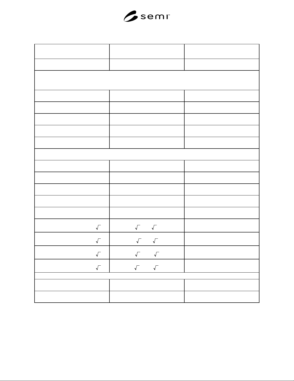
Table 2 Scan Pattern Locations
Location X, Y Coordinates
(per SEMI M20)
Scan Direction (for line and area
tools), parallel to:
Center Point 0, 0 Y-axis
5-point Pattern
Point # Location
1 Center Point 0, 0 Y-axis
2 2r/3 0, 2r/3 Y-axis
3 2r/3 -2r/3, 0 X-axis
4 2r/3 0, -2r/3 Y-axis
5 2r/3 2r/3, 0 X-axis
9-point Pattern
1Center0, 0 Y-axis
2 4r/5 0, 4r/5 Y-axis
3 4r/5 -4r/5, 0 X-axis
4 4r/5 0, -4r/5 Y-axis
5 4r/5 4r/5, 0 X-axis
6(r2 )/5 (r 2 )/5, (r 2 )/5
Y-axis
7(r2 )/5 - (r 2 )/5, (r 2 )/5
X-axis
8(r2 )/5 - (r 2 )/5, - (r 2 )/5
Y-axis
9(r2 )/5 (r 2 )/5, - (r 2 )/5
X-axis
Full FQA Scan
Raster Scan Full FQA X-axis
Concentric Circles or Spiral Full FQA
R – Theta
NOTE 1: r = nominal wafer radius
SEMI M40-0200 © SEMI 2000 10
Center Point *
Raster Scan
R-Theta
Five Point *
Nine Point *
11
7
8
9
6
4
4
2
2
333
5
5
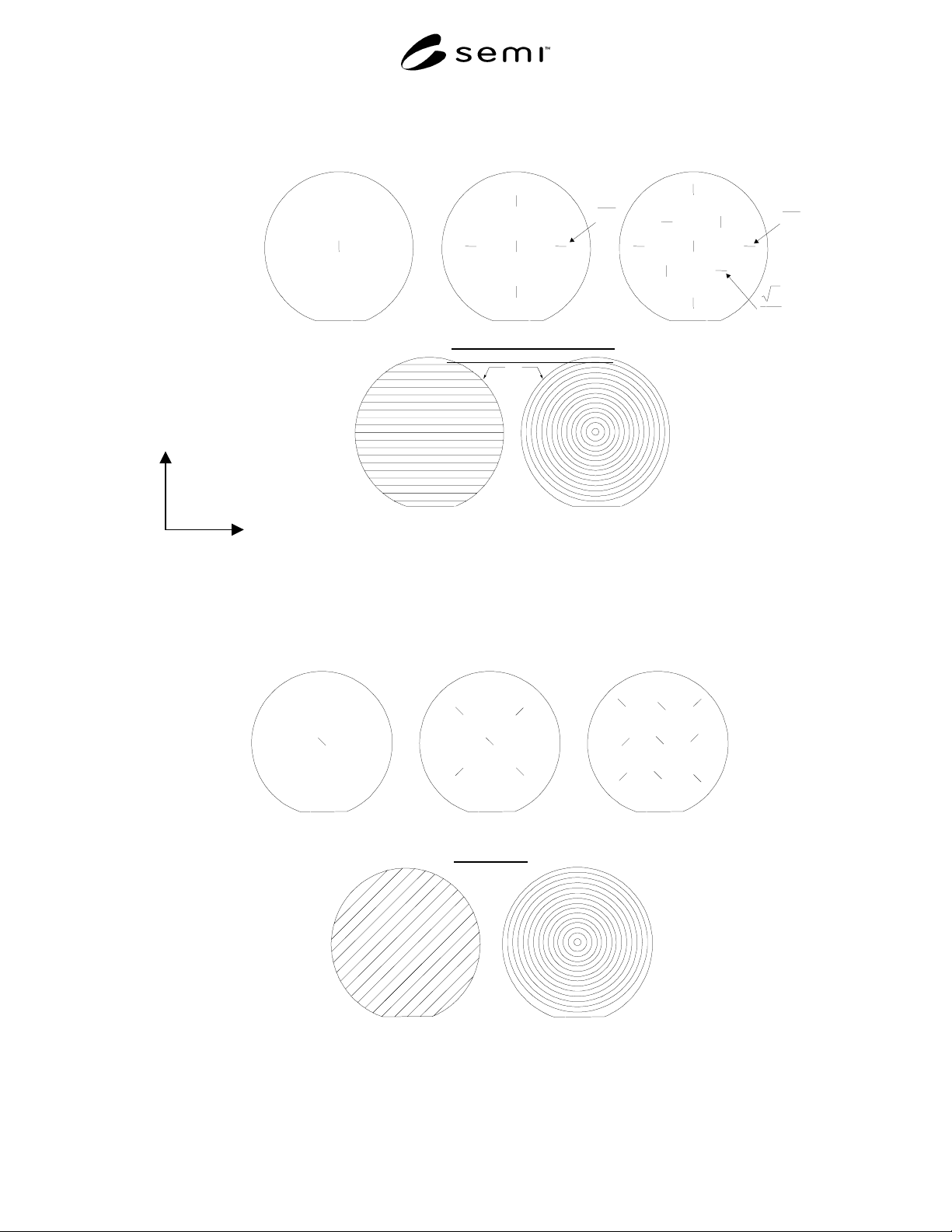
Type A Local Scan Patterns
*
* Line indicates scan direction for all line scans.
Centerpoint of line = location for point measurements
**
** Scan patterns to full FQA
2
3
r
4
5
r
2
5
r
Full FQA Scan Patterns
X
Y
Wafer and Scan
Coordinate System
Center Point
Five Point Nine Point
1
1
7
8
9
6
4
4
2
2
3
3
5
5
Raster Scan
R-Theta
Full FQA
Type B Local Scan Patterns
Figure 1
Patterns of Locations on a Silicon Wafer Surface for Measuring
(NOTE: R-Theta scan may be implemented in either a circular or a spiral pattern.)