semi合集-English.pdf - 第553页
SEMI E78-1102 © SEMI 1998, 2002 11 A1-2.2.1. 8 Using hig her values of N/A in Equati on 13 will increase the acceptable values of ct and m ax t . Accepting higher values of c will reduce max t . The guideline tabl e prov…
SEMI E78-1102 © SEMI 1998, 2002 10
recommendation (Table 1 in Section 12.5) – 50
nanocoulombs.
A1-2.1.4.3 Level 2 — Devices are damaged by lower
levels of static charge in equipment. Devices pass
testing at MM Class M1 (100 V × 200 picofarads = 20
nanocoulombs) and CDM Class C4 (1 kV × 10
picofarad device = 10 nanocoulombs). Guide
recommendation (Table 1 in Section 12.5) – 10
nanocoulombs.
A1-2.1.4.4 Level 1 — Devices are easily damaged by
even low levels of static charge in equipment. Devices
pass testing at CDM Class 1 (125 V × 10 picofarads
device = 1.25 nanocoulombs). In most cases simulator
equipment is not designed to do testing at these very
low levels for MM. Guide recommendation (Table 1 in
Section 12.5) – 1 nanocoulombs.
A1-2.2 Recommendations for Particle Deposition
A1-2.2.1 Related Information R1-2 discusses the
enhancement of particle deposition due to electrostatic
fields from charges on the wafer surface. This section
attempts to develop the guideline recommendations for
minimizing particle deposition based on that discussion.
A1-2.2.1.1 From Equation 3 of Related Information
R1-2.2,
N
/
A = cv
elect
t (12)
where N/A equals the particulate burden added to a
wafer during exposure time t, exposed to a particle
concentration c, in an environment characterized by an
electrostatic particle deposition velocity, v
elect
.
A1-2.2.1.2 Target values for N/A are given in the
National Technology Roadmap for Semiconductors
(NTRS, 1994). These target values vary from 0.02–0.01
defects/cm
2
, depending on the critical dimensions of the
technology, and represent an upper value of the
acceptable particulate concentration on a wafer at the
conclusion of the fabrication sequence. For individual
processing steps making up the fabrication sequence the
target values are lower yet.
A1-2.2.1.3 The variables c and t are process step
dependent and may or may not be controllable. Clearly
minimizing both of these variables is desirable in order
to minimize particle deposition on a wafer in any
environment.
A1-2.2.1.4 The only variable in Equation 12 that
depends on electrical forces is v
elect
. Both the particle
charge and the electric field in the vicinity of the wafer
affect the magnitude of v
elect
. Particle charge is
generally unknown unless it is deliberately controlled
by a neutralizing action, such as flooding the
environment with both positive and negative charges.
Under these conditions a Fuchs type charge distribution
is a reasonable assumption for the particle charge. This
assumption was used to calculate the values of E
0
in
Table R1-2 of Related Information R1-2.3.2.
A1-2.2.1.5 When the environmental electric field is
less than E
0
, deposition of electrically “neutralized”
particles is dominated by diffusion. When the
environmental electric field is greater than E
0
,
electrostatic forces dominate particle deposition even
when particle charge has been “neutralized.” Values of
E
0
for a Fuchs charge distribution can be calculated
from Related Information R1-2.3.2 Equation 10. For
particle charge greater than the Fuchs charge, v
elect
increases by a factor of q/q
Fuchs
. Unfortunately, the
actual particle charge q is generally unknown.
A1-2.2.1.6 Using the process step values of c and t and
the value of v
elect
calculated from Equation 10, the value
of N/A for any process step can be estimated.
Alternatively, having a target value of N/A and
estimating the value of v
elect
as outlined in the previous
paragraphs, allows one to calculate the tolerable value
of ct:
ct =[
N
/
A]
/
v
elect
(13)
A1-2.2.1.7 Setting N/A = 0.01/cm
2
and using Equation
10 to calculate v
elect
for a 0.1 µm particle at various
values of electric field and particle charge, target values
of ct can be calculated from Equation 13. The allowed
exposure times in an ISO Class 1 environment (c ≤ 10
-5
particles/cm
3
) can be deduced as shown in the
following table:
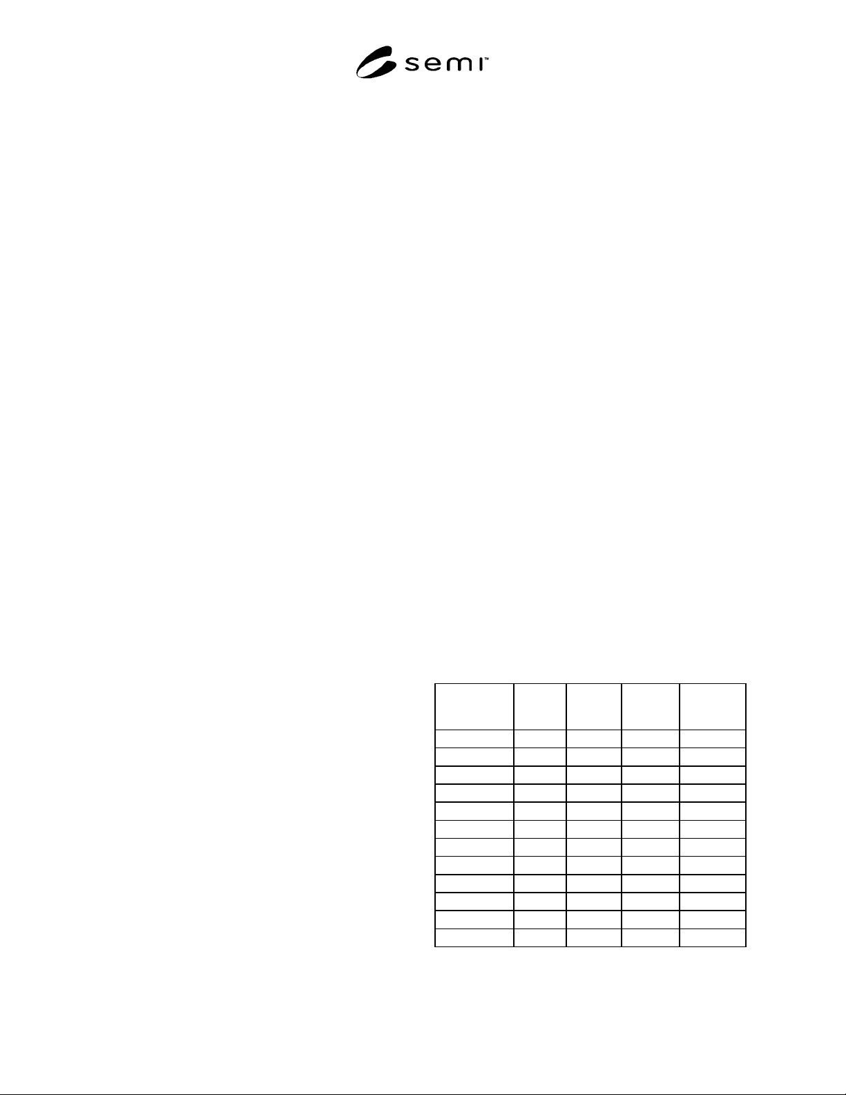
Table A1-1 Allowed Exposure Times in an ISO
Class 1 Environment
E V/cm at One
Wafer Radius
q/q
Fuchs
v
elect
cm/sec
ct sec/cm
3
max t in ISO
Class 1 sec
4000 1 0.8 0.01250 1250
2 1.6 0.00625 625
10 8.0 0.00125 125
400 1 0.08 0.1250 12500
2 0.16 0.0625 6250
10 0.8 0.0125 1250
200 1 0.04 0.250 25000
2 0.08 0.125 12500
10 0.4 0.025 2500
100 1 0.02 0.50 50000
2 0.04 0.25 25000
10 0.2 0.05 5000
SEMI E78-1102 © SEMI 1998, 2002 11
A1-2.2.1.8 Using higher values of N/A in Equation 13
will increase the acceptable values of ct and max t.
Accepting higher values of c will reduce max t. The
guideline table provides an order of magnitude
assessment of the degree of electric field and charge
control needed in specific operations. Minimum field
and minimum particle charge are always the goal but
usually not practically achievable. This guideline table
provides background estimates of envelopes for
acceptable operation in electrically charged
environments.
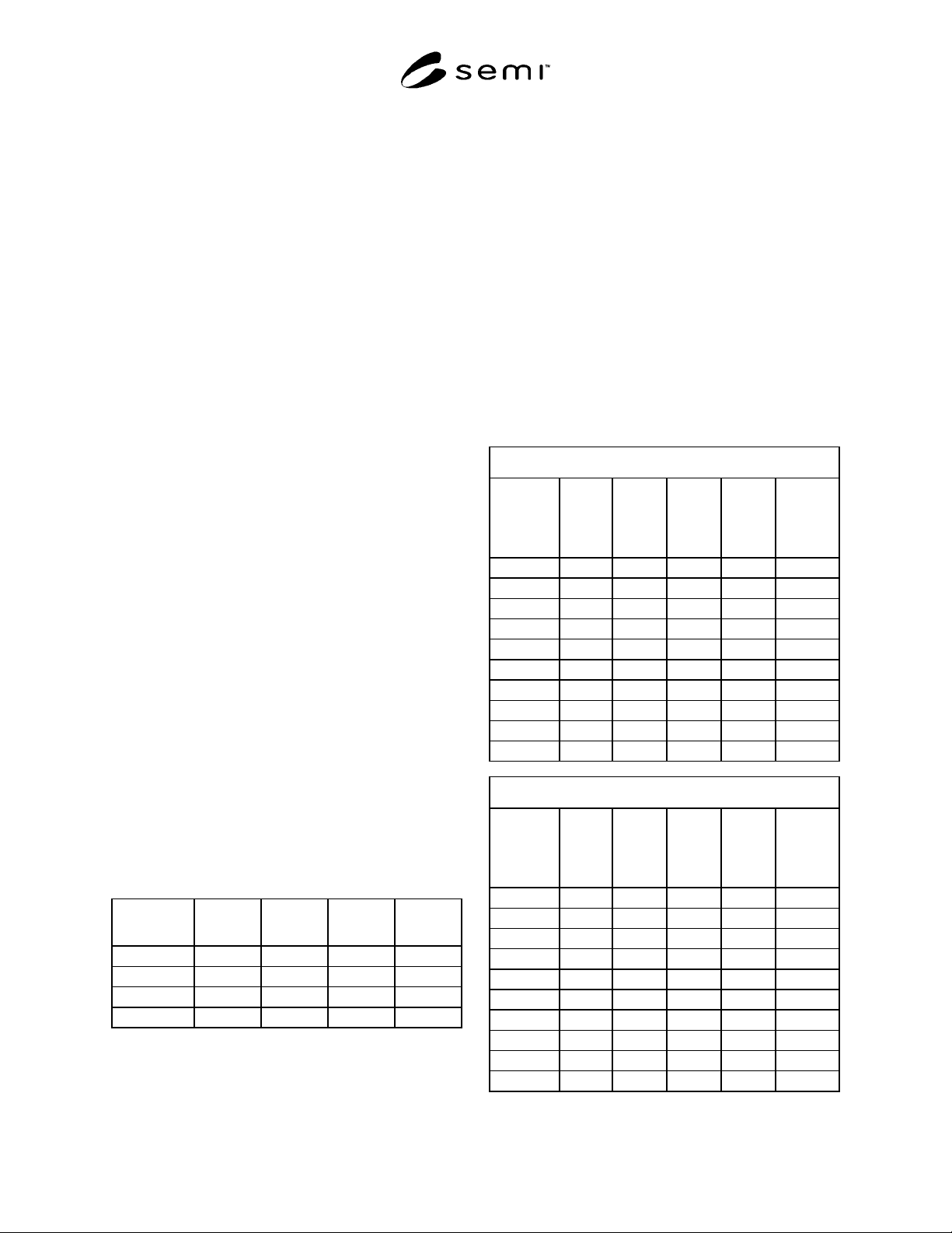
A1-2.2.2 The following simplified table is offered as
an alternative to Table A1-2 based on the following
assumptions:
1. Calculations made for Federal Standard 209E Class
1 (c ≤ 0.00124 particles/cm
3
).
2. The value of the electrostatic field is referenced at a
distance of one wafer radius from the wafer. While
electrostatic field measurements can certainly be
made at this distance, they are typically made at 2.5
cm (1 inch) with common instrumentation. This is
described in SEMI E43. Measurements made at this
smaller distance will be proportionally higher, but
under varying measurement conditions, it is difficult
to determine a precise relationship between electric
field and measurement distance. To provide a
suitable safety factor, assume a linear relationship,
rather than one proportional to the square of the
distance. For example, with a 200 mm wafer, 4000
Volts/cm at 2.5 cm would result in 1000 Volts/cm at
10 cm, rather than 250 Volts/cm.
3. The proportionality effect of q/q
Fuchs
has been
explained, as has the difficulty in actually
determining any value for it. For simplicity, the
table includes only the q = q
Fuchs
condition.
4. N/A = 0.016 defects/cm
2
as specified for 0.25 µm
technology in the National Technology Roadmap
for Semiconductors.
Table A1-2.1 Alternative to Allowed Exposure Times
in an ISO Class 1 Environment
EV/cm at 2.5
cm
N
/A defects
per cm
2
v
elect
cm/sec
ct
sec/cm
3
max t in
Class 1 sec
4000 0.016 0.21 0.0762 61
400 0.016 0.021 0.762 610
200 0.016 0.0105 1.524 1220
100 0.016 0.00525 3.048 2440
A1-2.3 Guide Recommendations for Equipment
Malfunctions
A1-2.3.1 Equipment Survey — Most semiconductor
production equipment should comply with the ESD
immunity requirements of the European Economic
Community (EEC). The testing mandated by the EEC
uses the test methods and ESD immunity levels
specified in IEC 6100-4-2. A recent survey of 262
semiconductor equipment suppliers revealed that 71%
were compliant with the EEC requirements. There is an
expectation that all equipment to be used in future 300
mm wafer fabrication will meet or exceed the ESD
immunity requirements of IEC 6100-4-2.
A1-2.3.1.1 To test for compliance, measurements were
made with the ESD simulator described by IEC 6100-4-
2 on a representative sample of semiconductor
equipment. The results were as follows:
ESD Simulator Testing Direct Contact Discharge
Equipment
Test
Voltage
Level 1
(2 kV)
Test
Voltage
Level 2
(4 kV)
Test
Voltage
Level 3
(6 kV)
Test
Voltage
Level 4
(8 kV)
Test
Voltage
Level X
(NOTE 1)
A X
B X
C X
D X
E X
F X
G X
H X
I X
J X
ESD Simulator TestingAir Discharge at 10 cm
Equipment Test
Voltage
Level 1
(2 kV)
Test
Voltage
Level 2
(4 kV)
Test
Voltage
Level 3
(8 kV)
Test
Voltage
Level 4
(15 kV)
Test
Voltage
Level X
(NOTE 1)
A X
B X
C X
D X
E X
F X
G X
H X
I X
J X
SEMI E78-1102 © SEMI 1998, 2002 12
“X” indicates that the equipment passes ESD simulator testing at this
level.
NOTE 1: This level is subject to negotiation and has to be
specified in the dedicated equipment specification. If higher
voltages than those shown are specified, special test
equipment may be needed.
A1-2.3.2 Static Audit — While equipment may meet
the ESD immunity levels specified in IEC 6100-4-2, it
should be remembered that static charge levels in
manufacturing environments may be substantially
higher. Direct measurements of static charge are
difficult, and the presence of a charge does not always
imply that an ESD event causing an equipment
malfunction will occur. Some information may be
gained by using a fieldmeter to measure the
electrostatic field created by the surface charge.
Instruments known as EMI locators may also be used in
some cases to determine if ESD-related EMI is
occurring. Some representative measurements of
electric fields from objects in various areas of a
semiconductor wafer fab are as follows:
• Wet Etch — 0.1 kV/inch to 30 kV/inch
• Planarization — 0.1 kV/inch to 20 kV/inch
• Lithography — 0.1 kV/inch to 20 kV/inch
• Dry Etch — 0.1 kV/inch to 15 kV/inch
• Thin Film — 0.1 kV/inch to 15 kV/inch
• Diffusion — 0.1 kV/inch to 30 kV/inch
• Implant — 0.1 kV/inch to 15 kV/inch
A1-2.3.2.1 A knowledge of object capacitance and
other physical properties is needed to determine if any
of the above measurements indicate an equipment
hazard due to ESD events. However, the range of the
measurements strongly indicate that such ESD events
can occur. The examples in Related Information R1-3.3
support this conclusion.
A1-2.3.3 Guide Recommendations — Based on the
static audits and equipment test data, there appears to be
a wide range of static immunity in equipment as well as
in the static charge levels in work environments. As
stated previously, it is difficult to establish a direct
correlation between ESD events and fieldmeter
measurements made on products, carriers, or any other
objects in the work environment. The following
sensitivity levels are defined with recommended test
levels for each.
A1-2.3.3.1 Level 4 — Field measurements of static
charge at input/exit ports are expected to exceed 10
kV/inch. Equipment should pass ESD simulator testing
at 8 kV direct contact discharge, 18 kV air discharge.
Guide recommendation (Section 12.5) - 1200
nanocoulombs (8 kV × 150 picofarads).
A1-2.3.3.2 Level 3 — Field measurements of static
charge at input/exit ports are expected to exceed 4
kV/inch, but are less than 10 kV/inch. Equipment
should pass ESD simulator testing at 4 kV direct
contact discharge, 8 kV air discharge. Guide
recommendation (Section 12.5) - 600 nanocoulombs (4
kV × 150 picofarads).
A1-2.3.3.3 Level 2 — Field measurements of static
charge at input/exit ports are expected to exceed 500
V/inch, but are less than 4 kV/inch. Equipment should
pass ESD simulator testing at 2 kV direct contact
discharge, 4 kV air discharge. Guide recommendation
(Section 12.5) - 300 nanocoulombs (2 kV × 150
picofarads).
A1-2.3.3.4 Level 1 — Field measurements of static
charge at input/exit ports are expected to exceed zero,
but are less than 500 V/inch. Equipment should pass
ESD simulator testing at 1 kV direct contact, 2 kV air
discharge. Guide recommendation (Section 12.5) - 150
nanocoulombs (1 kV × 150 picofarads).
NOTICE: SEMI makes no warranties or
representations as to the suitability of the standards set
forth herein for any particular application. The
determination of the suitability of the standard is solely
the responsibility of the user. Users are cautioned to
refer to manufacturer’s instructions, product labels,
product data sheets, and other relevant literature
respecting any materials mentioned herein. These
standards are subject to change without notice.
The user’s attention is called to the possibility that
compliance with this standard may require use of
copyrighted material or of an invention covered by
patent rights. By publication of this standard, SEMI
takes no position respecting the validity of any patent
rights or copyrights asserted in connection with any
item mentioned in this standard. Users of this standard
are expressly advised that determination of any such
patent rights or copyrights, and the risk of infringement
of such rights, are entirely their own responsibility.