semi合集-English.pdf - 第6010页
SEMI G1-96 © SEMI 1 980, 199 6 3 5.19 void — An ab sence of metalliz a ti on o r glass from a design ated metallized or glassed area on a ceramic surface. 6 Orderi ng Information Purchas e orders for cerdip com ponents o…
SEMI G1-96 © SEMI 1980, 1996 2
5.3 camber (ceramic) — Arching of a nominally flat
ceramic body.
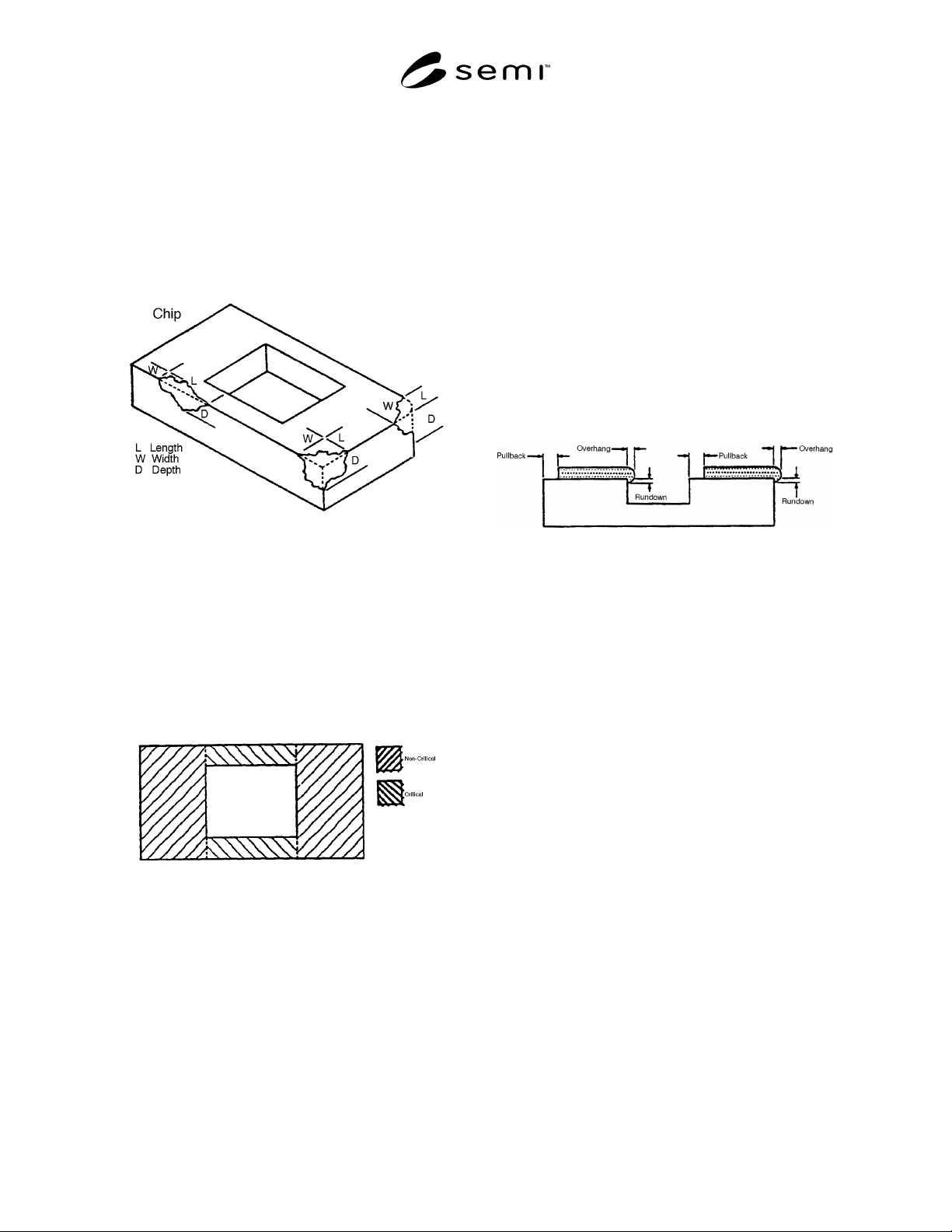
5.4 chip — A region of material missing from a
component (e.g., ceramic from a package, or solder
from a preform). The region does not progress
completely through the component and is formed after
the component is manufactured. Chip size is defined by
its length, width, and depth from a projection of the
design planform. Also called chipout (see Figure 1).
Figure 1
5.5 crack — A cleavage or fracture that extends to the
surface of a semiconductor package or solder
preform.The crack may or may not pass through the
entire thickness of the package or preform.
5.6 critical seal area — On a semiconductor package,
the area bounded by the shortest nominal design
distance from the largest cavity, usually the wire bond
cavity, to the edge of the package or ceramic layer
forming the seal area (see Figure 2).
Figure 2
Critical and Non-Critical Seal Area
5.7 fin — On a ceramic package or cap, a fine
feathery-edged projection of parent ceramic material on
the corner of the ceramic body.
5.8 foreign material — An adherent particle that is not
parent material of the component. Adherence means
that the particle cannot be removed by an air or nitrogen
blast at 20 psi.
5.9 glass flow — On a semiconductor package or cap,
the heating process which just removes all the screen
printing mesh marks in the sealing glass when viewed
at 10× magnification.
5.10 glass void — The absence of a sealing glass layer
from a designated area.
5.11 metallization void — The absence of a clad,
evaporated, plated, or screen-printed metal layer or
braze from a designated area.
5.12 non-critical seal area — On a semiconductor
package that uses a lid, cap, or cover to effect the seal,
the area of the sealing surface outside the critical
sealing area (see Figure 2).
5.13 overhang — On a semiconductor package, the
horizontal extension of the sealing glass past the
vertical wall of a cavity cut into the ceramic layer on
which the glass is printed (see Figure 3).
Figure 3
Glass Misalignment
5.14 peeling (flaking) — Any separation of a plated,
vacuum-deposited, or clad metal layer from the base
metal of a leadframe, pin heatsink, or seal ring, from an
underplate or from a refractory metal on a ceramic
package. Peeling exposes the underlying metal.
5.15 projection — On a semiconductor package
(plastic or ceramic) leadframe or preform, an irregularly
raised portion of a surface indigenous to the parent
material.
5.16 pullback — On a semiconductor package, the
linear distance between the edge of a cavity cut into a
ceramic layer and the first measurable glass or
metallization layer interface coated onto the top surface
of that layer. The total pullback may be the result of the
high-temperature processing required to manufacture
the package or to coat the surface. It may also be the
result of design considerations (see Figure 3).
5.17 rundown — On a semiconductor package, the
linear distance from the upper surface of a ceramic
cavity layer to the bottom point of the overhang into the
cavity, of a sealing glass or metallization layer that has
been screened onto that surface (see Figure 3).
5.18 seal area — On a semiconductor package, the
area designated for sealing a cover or lid to a cofired
ceramic package, to a cap to a cer-pack base.

SEMI G1-96 © SEMI 1980, 19963
5.19 void — An absence of metallization or glass from
a designated metallized or glassed area on a ceramic
surface.
6 Ordering Information
Purchase orders for cerdip components or sub-
assemblies furnished to this specification shall include
the following items:
6.1 Current drawing revision detai ling:
6.1.1 All dimensions and tolerances per ANSI
Y14.5M practices
6.1.2 Type and color of ceramic
6.1.3 Type and thickness of glass
6.1.4 Type and thickness of die pad metallization
NOTE 3: If sub-assemblies are purchased, the leadframe
details shall be as described in SEMI G2. In some cases,
unlike the frames described in SEMI G2, the leadframes may
also have a die-attach pad. If required, the external lead
plating requirements for these sub-assemblies shall also be
specified. (See SEMI G20 for general details of lead finishes.)
If sub-assemblies are purchased, leadframe inspection shall
follow the requirements detailed in Section 9.
6.2 Incoming Inspection and Functional Tests — See
Sections 9 and 10.
6.3 Incoming Sampling Procedures — See Section 11.
6.4 Packaging and Marking Requirements — See
Section 12.
6.5 Vendor Certification Requirements — See Section
13.
6.6 Any additions to, or variations from, this
specification.
7 Dimensions
The components or sub-assemblies described in this
specification shall produce packaged devices that
conform to the outline dimensions and lead numbering
for cerdip package constructions detailed in:
— JEDEC Publication 95 and
— MIL-STD-1835.
Package manufacturing tolerances shall be agreed upon
between user and supplier and detailed in the drawings.
Typical dimensions and tolerances for standard bases
and caps are shown in the appendices at the end of this
specification.
8 Materials
The definitions defect criteria and functional tests
described in this specification relate to package
components made with the following materials:
8.1 Bases, Window Frames, and Caps
8.1.1 Material — Ceramic with 90% alumina,
minimum content.
8.1.2 Color — Black, dark brown, or dark violet.
8.2 Sealing Material
8.2.1 Material — Solder glass desig ned to seal metal
(typically Iron-Nickel-Cobalt alloy per MIL-M-38150,
Type A or Iron-Nickel alloy per MIL-M-38150 Type B)
to ceramic.
8.3 Die-Attach Pad
8.3.1 Material — Thick film gold or other specified
material.
8.4 Leadframe
8.4.1 Leadframes, whether purchased as component or
in sub-assemblies, shall conform to the requirements of
SEMI G2 as required.
9 Defect Limits
The following defects shall be cause for rejection if the
limits shown are exceeded:
NOTE 4: The criteria apply to purchased components and
pre-assemblies, as applicable, or, where applicable, to units
assembled by the user to process conditions agreed upon
between the user and supplier.
9.1 Ceramic Components
9.1.1 Cracks — Any crack.
9.1.2 Chips — See Figures 1 and 2.
9.1.2.1 Corner Chips — 0.030" (0.762 mm) × 0.030"
(0.726mm) × 25% of the package element thickness.
9.1.2.2 Edge Chips — 0.100" (2.54 mm) × 0.030"
(0.726mm) × 25% of the package element thickness.
9.1.2.3 Critical Seal Area — Chips shall not reduce
the critical seal path, at any point, more than 30%. No
more than four chips are allowed in this area, regardless
of loss of seal length.
9.1.3 Burrs, Projection (Fins), and Blisters
9.1.3.1 Bases, Caps, and Window Frames — 0.005"
(0.127 mm) maximum allowable dimension in the plane
of the component, or greater than 0.003" (0.076 mm) in
height.
SEMI G1-96 © SEMI 1980, 1996 4
9.1.3.2 Die-Attach Surface (on Base Ceramic) — 0.005" (0.127 mm) dimension in the plane of the component, or
greater than 0.001" (0.254 mm) above the surface of the metallization excluding a zone, 0.010" (0.254 mm) wide,
around the periphery of the cavity.
9.1.4 Camber — Shall be agreed upon between user and supplier and specified on the component or sub-assembly
drawing. Standard limits shall be 0.003"/inch (0.003 mm/mm), maximum, with a minimum allowable camber of
0.002" (0.051 mm).
9.1.5 Foreign Material — 0.020" (0.508 mm) maximum allowable surface dimension or 0.005" (0.127 mm) in
height. No more than three sites allowed and a minimum separation of 0.030" (0.762 mm) between sites.
9.2 Glass Sealant
9.2.1 Chips and Voids — 0.010" (0.025 mm) maximum allowable dimension. In the critical seal, there shall be no
more than four acceptable chips or voids. In critical and non-critical seal areas, there shall be no voids after a glass
flow cycle.
9.2.2 Glass Misalignment — (After glass flow on components, see Figure 3, or on sub-assemblies.)
9.2.2.1 Glass Overhang — 0.015" (0.381 mm) maximum extension from the ceramic edge.
9.2.2.2 Glass Rundown — 50% of the package element thickness.
9.2.2.3 Glass Rundown into the Die-Attach Cavity — 0.010" (0.254 mm) maximum extension from the ceramic
surface into the cavity.
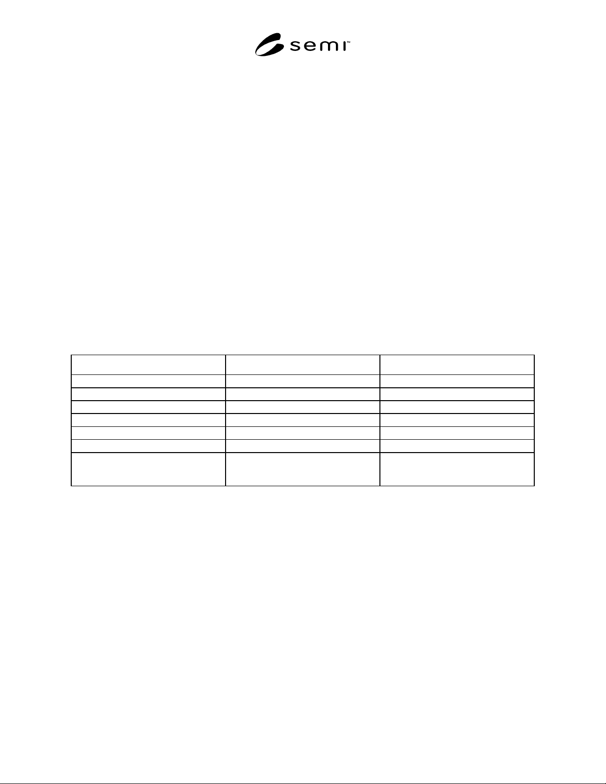
9.2.2.4 Glass Pullback (After Glass Flow) — See Table 1 and Figure 3.
Table 1 Maximum Allowable Pullback
Area of Package Package Row Spacing Package Row Spacing
0.300" (7.500 mm) and 0.400"(10.16 mm) 0.600" (15.24 mm) and larger
Side external (critical seal area) 0.010" (0.254 mm) 0.015" (0.381 mm)
Side external (non-critical seal area) 0.015" (0.381 mm) 0.015" (0.381 mm)
End external 0.020" (0.508 mm) 0.020" (0.508 mm)
Side cavity 0.010" (0.254 mm) 0.015" (0.381 mm)
End cavity 0.010" (0.254 mm) 0.015" (0.381 mm)
Maximum allowable critical seal length
reduction on any one side, as measured
between the cavity and the external side
0.015" (0.381 mm) 0.020" (0.508 mm)
NOTE 5: Regardless of the maximum criteria noted in Table 1, the critical seal length at any point shall not be reduced any more
than 30%.
9.2.2.5 Foreign Material — 0.020" (0.508 mm) maximum allowable surface dimension in the plane of the glass,
but 0.010" (0.254 mm) in the critical seal area, with no more than three sites allowed and a minimum separation of
0.030" (0.762 mm) between sites.
9.3 Die-Attach Cavity Metallization (0n Ceramic Base) — Excluding a 0.010" (0.254 mm) wide zone around the
periphery of the cavity, the following criteria shall apply:
9.3.1 Foreign Material, Including Glass Splatters — 0.005" (0.130 mm) maximum in the plane of the metallization
or greater than 0.001" (0.025 mm) in height with no more than three sites allowed and a minimum separation of
0.030" (0.763 mm) between sites.
9.3.2 Metallization Nodules — No more than three allowed. If the metallization is gold and gold-silicon eutectic die
attach is to be used, the bumps may not exceed 0.010" (0.254 mm) in the surface dimension or 0.005" (0.130 mm) in
height. If silver glass or resin bonding is to be used, the nodules shall be treated as foreign material per Section 9.3