semi合集-English.pdf - 第6227页
SEMI G46-88 © SEMI 1988 4 The usual r ule of thumb in setting the maxi mum limit for ∆ V F or CU is to use the distribution average value and one s tandard deviat ion ( σ ) i.e. — ( ∆ V F ) high limit =∆ V F + X σ ∆ (CU)…

SEMI G46-88 © SEMI 19883
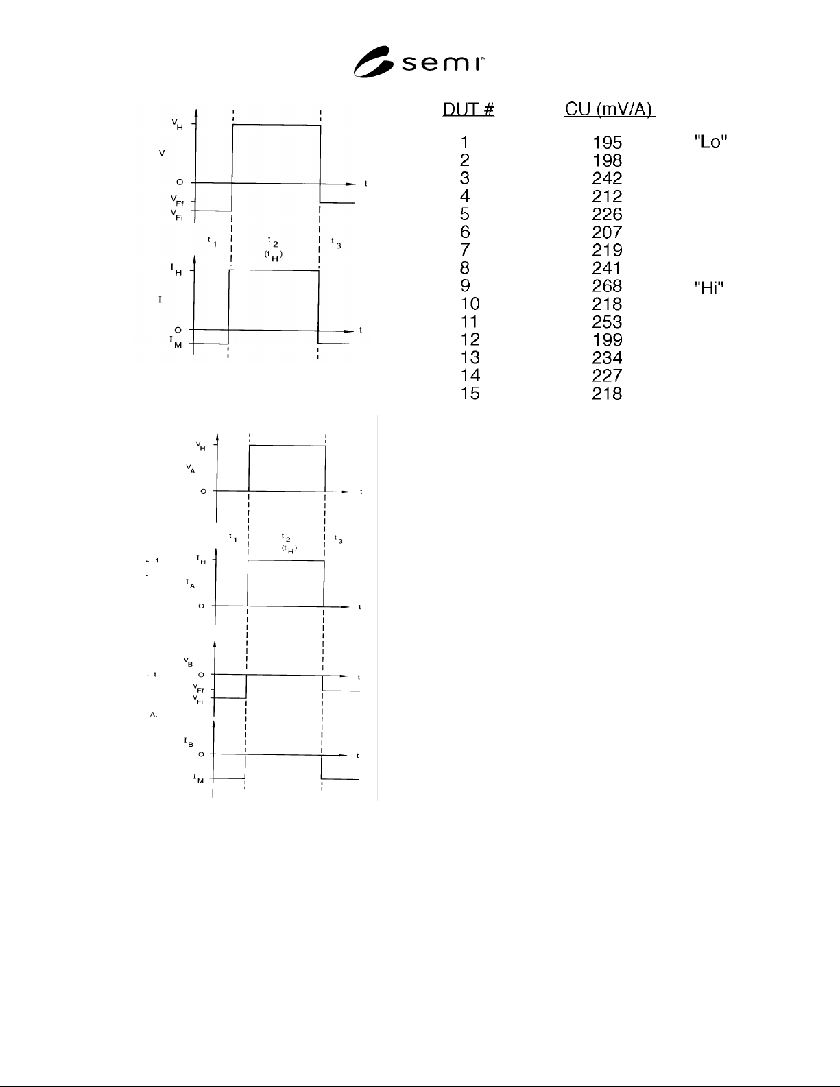
Step 4 — Test each of the sample devices and record
the ∆V
F
and CU data as shown in Figure 3.
Step 5 — Select out the devices with the highest and
lowest values of CU and put the remaining devices
aside.
The ∆V
F
values can be used instead of CU if the mea-
sured values of I
H
are very tightly grouped aroung the
average value.
Step 6 — Following the Heating Time (t
H
) sequence
shown in Figure 4, read and record the ∆V
F
and CU
data values for each of the two devices of Step 5.
Step 7 — Using the data from the previous step,
prepare heating curves for the two devices in a manner
similar to the examples shown in Figure 5.
Step 8 — Interpretation of the heating curves is the next
step. Realizing that the thermal characteristics of
identical chips should be the same if the heating time
(t
H
) is less than or equal to the thermal time constant of
the chip, the two curves should start out the same for
the low values of t
H
. Non-identical chips (i.e., thinner or
smaller in cross section) will have completely different
curves, even at the smaller values of t
H
. As the value of
t
H
is increased, thereby overcoming the chip thermal
constant, heat will have propagated through the chip
into the die attachment region. Since the heating curve
devices of Step 5 were specifically chosen for their
difference, the curves of Figure 5 diverge after t
H
reaches a value where the die attachment variance has
an effect on the device junction temperature. Increasing
t
H
further will probably result in a flattening of the
curve as the heating propagates in the device package.
If the device package has little thermal mass and/or is
not well mounted to a good heat sink, the curve will not
flatten very much, but will show a definite change in
slope. Figure 6 shows the key elements of the heating
curve.
Step 9 — Using the heating curve, select the
appropriate value of t
H
to correspond to the inflection
point in the transition region between heat in the chip
and heat in the package.
If there are several different elements in the heat flow
path-chip, die attachment, substrate, substrate
attachment, and package, for example, in a hybrid there
will be several plateaus and transitions in the heating
curve. Appropriate selection of t
H
will optimize
evaluation sensitivity to other attachment areas.
Step 10 — Return to the apparatus and set t
H
equal to
the value determined from Step 9.
Step 11 — Because the selected value of t
H
is much less
than that for thermal equilibrium, it is possible to
significantly increase the heating power without
degrading or destroying the device. The increased
power dissipation within the device under test will
result in high ∆V
F
and/or CU values that will make
determination of acceptable and non-acceptable devices
much easier.
Step 12 — The pass/fail limit, the cutoff point between
acceptable and non-acceptable devices, can be
established in a variety of ways:
a) Correlation to other die attachment evaluation
methods, such as die shear and/or x-ray; while these
two methods have little actual value from a thermal
point of view, they do represent standardized methods
as described in MIL-STD specifications.
b) Maximum allowable junction temperature variation
between devices; since the relationship between ∆T
J
and ∆V
F
is about 0.5°C/mV, the junction temperature
spread between devicescan be easily determined. The
T
J
predicts reliability. Conversely, the T
J
spread neces-
sary to meet the reliability projections can be translated
to a ∆V
F
and/or CU value for a Pass/Fail criteria, based
on correlation with steady-state thermal equilibrium
conditions.
To fully use this approach, it will be necessary to
calibrate the devices for the exact value of the T
J
- V
F
characteristic. The characteristic’s slope, commonly
referred to as K Factor, is easily measured on a sample
basis using a voltmeter, environmental chamber,
temperature indicator and a power supply setup for
forcing, both active devices and thermal test chips as
shown in Figure 7. A simple set of equations yields the
junction temperature once K and ∆V
F
are known:
∆T
j
= | (K) (∆V
F
) |
T
J
= T
A
+ ∆T
j
Where T
A
is the ambient or reference temperature.
c) Statistically from a moderate size device sample; the
distribution of ∆V
F
or CU values should be a normal
one with defective devices out of the normal range.
Figure 8 shows a ∆V
F
distribution for a sample lot of
integrated ciruits. Note that the left-hand side of the
histogram envelope is fairly well-defined, but the other
side is greatly skewed to the right. This comes about
because the left-hand side is constrained by the
absolutely best heat flow that can be obtained with a
given chip assembly material and process. The other
side has no such constraints because there is no limit as
to how poorly a chip is mounted.
SEMI G46-88 © SEMI 1988 4
The usual rule of thumb in setting the maximum limit
for ∆V
F
or CU is to use the distribution average value
and one standard deviation ( σ) i.e. —
(∆V
F
)
high
limit
=∆V
F
+ X
σ
∆
(CU)
high
limit
= CU + X
σ
CU
Where X = 1 in most cases.
The statistical data required is obtained by testing 40 or
more devices under the conditions of Step 11.
Step 13 — Once the test conditions and pass/fail limit
have been determined, it is necessary only to record this
information for future testing requirements of the same
device in the same package. With the apparatus
properly set-up, including the fail limit selector on
those apparatus set ups so equipped, the operator need
only insert the device, initiate a test, and then either
read the ∆V
F
or CU display or observe the appropriate
pass or fail indicaors.
The steps listed hereto have been conveniently
summarized in Figure 9. The total time required to
perform these steps is greatly dependent on the operator
but, in general, should require about one hour if the
statistical approach of Step 12.C is used.
4.2
Routine Device Testing Proced ure — Once the
proper control settings have been determined for a
particular device type from a given manufacturing
process or vendor, repeated testing of that device type
simply requires that the same test conditions be used as
previously determined.
New device types or the same devices manufactured
with a different process will require a repeat of Section
4.1.
4.3
Comparison of Different Vend or Devices — Each
device type is defined as a specific chip manufactured
to a given set of procedures. Integrated circuit users
who buy a specific part number from more than one
vendor or manufacturers that redesign or otherwise
modify the fabrication of their devices will be able to
use the heating power and approximately the same t
H
for all vendors, but probably will have to use a different
∆V
F
or CU pass/fail limit for each different vendor
because the K Factor for parts manufactured by
different vendors will probably be different. The
difference can be determined in Step 12.B and using the
setup described in Figure 7.
5 Test Condition Specification
To properly set up the test apparatus and to insure
repeatable measurements, the following test conditions
must be fully specified:
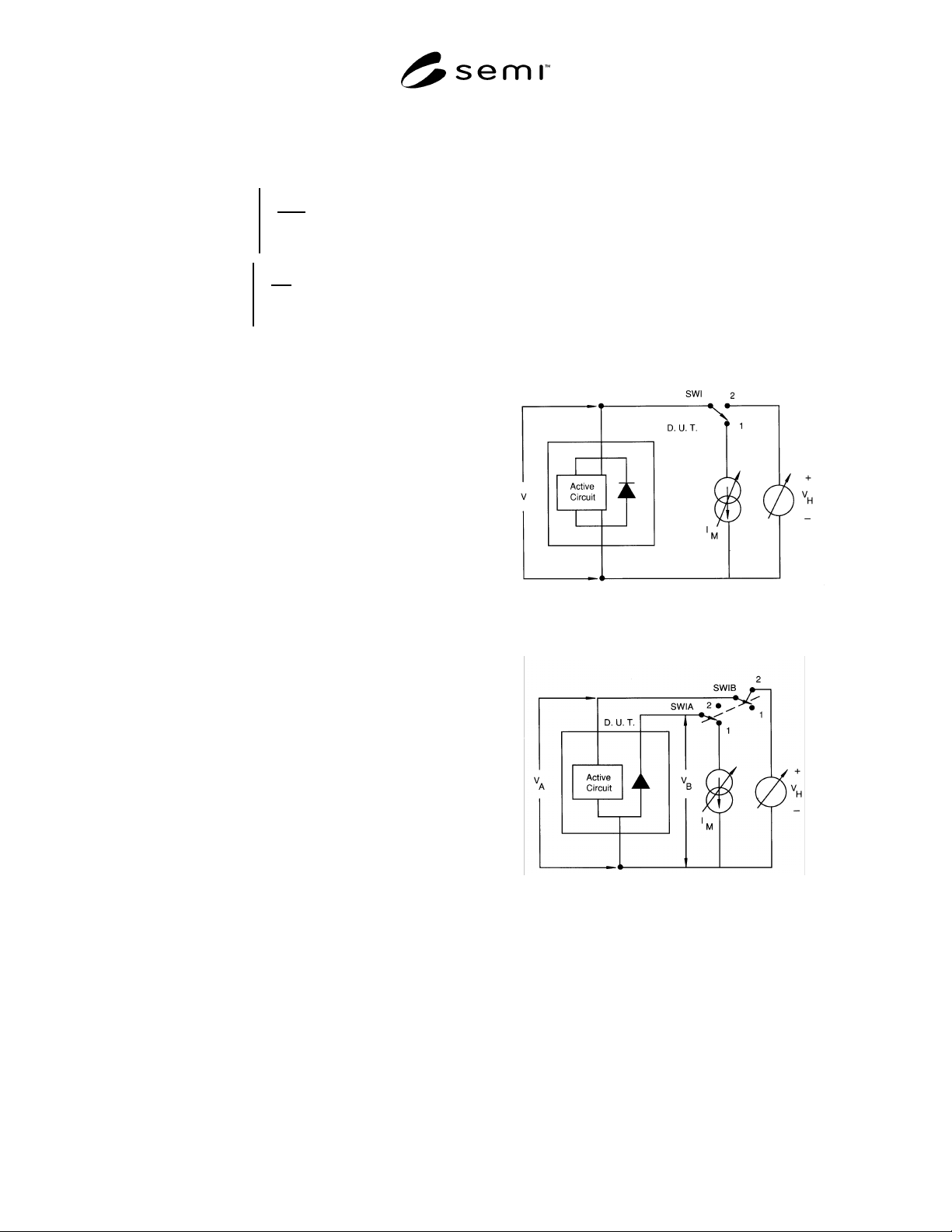
a. V
H
b. t
H
c. I
M
d. t
MD
(and t
SW
if appropriate)
e. DUT/apparatus interface (i.e., wiring connection)
f. ∆V
H
or CU data requirement
Figure 1A
Set-Up for Junction Isolation Diode Devices
Figure 1B
Set-Up for Parisitic Diode or Thermal Test Chip
Temperature Sensing
SEMI G46-88 © SEMI 19885
Figure 2A
Waferforms Associated with Figure 1A
Figure 2B
Waferforms Associated with Figure 2B
Figure 3
Data Results for Initial 15-Piece Sample for tH
Value of 200 ms